QFN11T
QFN sockets with 0.5mm pitch for various pin configurations
Manufacturer: yamaichi
series introduction
# QFN11T Product Series Introduction
## 1. Overview
The QFN11T product series represents a cutting - edge advancement in semiconductor packaging technology. QFN, which stands for Quad Flat No - lead, is a well - known and widely used surface - mount package type. The "11T" in the QFN11T series indicates specific characteristics and dimensions that make this product series suitable for a variety of high - performance applications.
## 2. Physical Characteristics
### 2.1 Package Design
- **Leadless Design**: The QFN11T features a leadless package, which offers several advantages over traditional leaded packages. The absence of leads reduces the package's footprint on the printed circuit board (PCB), allowing for more compact and space - efficient designs. This is particularly crucial in modern electronic devices where miniaturization is a key trend.
- **Quad Flat Shape**: The quad flat shape of the package provides a symmetrical structure, which simplifies the PCB layout and soldering process. It also ensures uniform heat dissipation and electrical performance across the package.
### 2.2 Dimensions
The specific dimensions of the QFN11T series are precisely engineered to meet industry standards and application requirements. The package has a well - defined length, width, and height, which are optimized for compatibility with automated pick - and - place equipment used in high - volume manufacturing. The small form factor of the QFN11T makes it ideal for use in portable devices, such as smartphones, tablets, and wearables.
### 2.3 Terminal Configuration
The QFN11T series has a specific terminal configuration that is designed to provide reliable electrical connections. The terminals are located on the bottom of the package and are arranged in a pattern that allows for efficient signal routing on the PCB. The terminal design also helps to minimize electrical interference and crosstalk, ensuring high - quality signal transmission.
## 3. Electrical Performance
### 3.1 Low Resistance and Inductance
The leadless design of the QFN11T significantly reduces the resistance and inductance of the electrical connections. This results in lower power losses and improved signal integrity, especially at high frequencies. The low inductance also helps to reduce electromagnetic interference (EMI), making the QFN11T suitable for use in sensitive electronic systems.
### 3.2 High - Speed Signal Handling
The QFN11T series is capable of handling high - speed signals with minimal distortion. This makes it an excellent choice for applications such as high - speed data communication, where fast and accurate signal transmission is essential. The package's electrical characteristics are optimized to support data rates in the gigahertz range.
### 3.3 Power Efficiency
The low resistance and inductance of the QFN11T contribute to its high power efficiency. By reducing power losses, the package helps to extend the battery life of portable devices and reduces the overall energy consumption of electronic systems. This is an important consideration in today's energy - conscious world.
## 4. Thermal Performance
### 4.1 Efficient Heat Dissipation
The QFN11T series is designed to provide efficient heat dissipation. The large exposed pad on the bottom of the package acts as a heat sink, allowing heat to be transferred directly from the semiconductor die to the PCB. This helps to keep the device operating at a lower temperature, which improves its reliability and performance.
### 4.2 Thermal Resistance
The thermal resistance of the QFN11T is carefully engineered to ensure optimal heat transfer. The package's design minimizes the thermal resistance between the die and the ambient environment, allowing for effective cooling even in high - power applications.
## 5. Applications
### 5.1 Consumer Electronics
In consumer electronics, the QFN11T series is widely used in smartphones, tablets, and smart
Images for reference
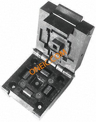
Image Preview
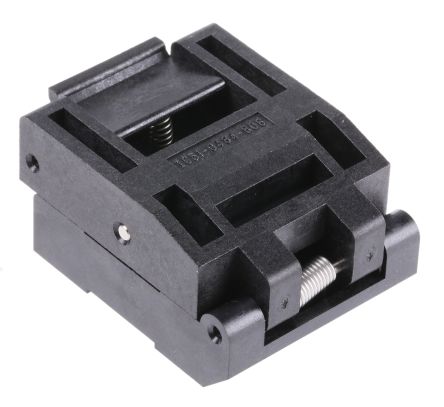
Image Preview
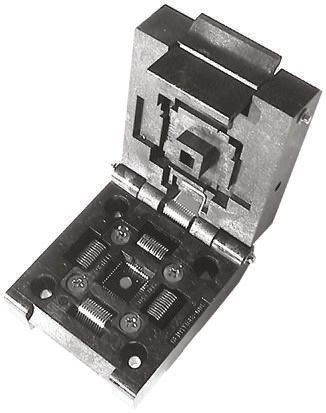
Image Preview