PI6C48545
3.3V low skew clock buffers and drivers for signal distribution
Manufacturer: ['diodes', 'pericom']
series introduction
# PI6C48545 Product Series Introduction
## 1. Overview
The PI6C48545 product series is a cutting - edge offering in the field of timing and clock management solutions. Developed by a leading semiconductor company, these devices are engineered to meet the stringent requirements of modern electronic systems, providing high - performance, reliable, and flexible clock generation and distribution capabilities.
## 2. Key Features
### 2.1 High - Precision Timing
- The PI6C48545 series is equipped with advanced phase - locked loop (PLL) technology. This allows for the generation of highly accurate clock signals with extremely low jitter. Jitter, which is the variation in the timing of a clock signal, can have a significant impact on the performance of digital circuits. With low jitter, these devices ensure that data is transferred and processed accurately, reducing the likelihood of errors in high - speed communication systems, such as Ethernet, USB, and PCIe.
- The frequency synthesis capabilities of the PI6C48545 are highly flexible. It can generate a wide range of output frequencies, from a few megahertz to several gigahertz, enabling it to support a diverse set of applications.
### 2.2 Multiple Outputs
- These devices offer multiple clock outputs, typically up to 8 or more. This feature is extremely useful in complex electronic systems where multiple components require different clock signals. For example, in a server motherboard, different chipsets, such as the CPU, GPU, and memory controllers, may need specific clock frequencies. The PI6C48545 can generate and distribute these different clock signals simultaneously, simplifying the overall clock management design.
- The outputs can be configured independently, allowing for different output drive strengths, signal levels (such as LVCMOS, LVDS), and phase relationships. This flexibility enables seamless integration with a variety of downstream components.
### 2.3 Programmability
- The PI6C48545 series is highly programmable, which is a major advantage in today's rapidly evolving electronic market. Through an I2C or SPI interface, users can easily configure various parameters of the device, such as output frequencies, phase shifts, and output enable/disable settings.
- This programmability allows for quick customization of the clock solution to meet the specific requirements of different applications. For example, in a product development cycle, engineers can easily adjust the clock settings during testing and optimization phases without having to change the hardware design.
### 2.4 Low Power Consumption
- In an era where energy efficiency is a top priority, the PI6C48545 series is designed to consume minimal power. This is achieved through advanced circuit design techniques and the use of low - power semiconductor processes.
- Low power consumption not only reduces the overall energy cost of the system but also helps in heat management. In compact electronic devices, excessive heat can lead to performance degradation and reliability issues. By consuming less power, the PI6C48545 helps in maintaining a stable operating temperature.
### 2.5 Robustness and Reliability
- These devices are built to withstand harsh operating conditions. They have a wide operating temperature range, typically from - 40°C to 85°C, making them suitable for use in industrial, automotive, and aerospace applications.
- The PI6C48545 series also features built - in protection mechanisms against electrostatic discharge (ESD) and electrical overstress (EOS). This ensures the long - term reliability of the device and reduces the risk of damage during handling and operation.
## 3. Applications
### 3.1 Data Centers
- In data centers, high - speed and accurate clock signals are crucial for the proper functioning of servers, storage systems, and networking equipment. The PI
Images for reference
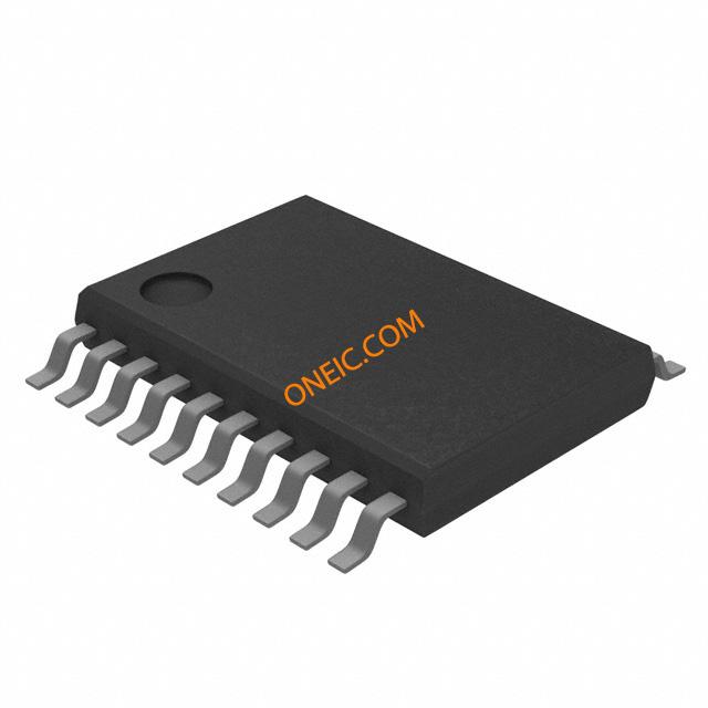
20-TSSOP
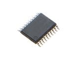
Image Preview