OMAP3525ECUS
ARM Cortex-A8 application processors in 423-pin BGA format
Manufacturer: ti
series introduction
# Introduction to the OMAP3525ECUS Product Series
## 1. Overview
The OMAP3525ECUS product series represents a significant advancement in embedded processing technology. Developed by Texas Instruments, these devices are engineered to meet the diverse and demanding requirements of a wide range of embedded applications. The OMAP3525ECUS combines high - performance computing capabilities with low power consumption, making it an ideal choice for applications where both processing power and energy efficiency are crucial.
## 2. Key Features
### 2.1 Processor Core
- **ARM Cortex - A8 Core**: At the heart of the OMAP3525ECUS is a powerful ARM Cortex - A8 processor core. This core operates at speeds up to 600 MHz, providing excellent processing performance for running complex operating systems and applications. The ARM Cortex - A8 architecture offers advanced features such as a superscalar pipeline, which allows for the simultaneous execution of multiple instructions, and a large cache memory system to reduce memory access latency.
- **NEON Multimedia Extension**: The inclusion of the NEON multimedia extension in the ARM Cortex - A8 core enables efficient processing of multimedia data. This extension provides a set of SIMD (Single Instruction, Multiple Data) instructions that can perform parallel operations on multiple data elements simultaneously. As a result, the OMAP3525ECUS can handle tasks such as video decoding, image processing, and audio encoding with high efficiency.
### 2.2 Graphics Processing Unit (GPU)
- **PowerVR SGX530 GPU**: The OMAP3525ECUS is equipped with a PowerVR SGX530 GPU. This GPU is capable of delivering high - quality 2D and 3D graphics performance. It supports OpenGL ES 2.0 and OpenVG 1.1 standards, which are widely used in the development of mobile and embedded graphics applications. The GPU can handle complex graphical user interfaces (GUIs), 3D games, and video playback with smooth and realistic visuals.
### 2.3 Memory and Storage
- **Memory Interfaces**: The device features multiple memory interfaces, including DDR2 SDRAM and NAND Flash interfaces. The DDR2 SDRAM interface allows for high - speed data transfer between the processor and the external memory, enabling fast application loading and execution. The NAND Flash interface provides a reliable and cost - effective solution for storing large amounts of data, such as the operating system, application code, and user data.
- **On - Chip Memory**: In addition to the external memory interfaces, the OMAP3525ECUS also has on - chip memory, including a Level 1 (L1) cache and a Level 2 (L2) cache. The L1 cache provides fast access to frequently used data and instructions, while the L2 cache acts as a larger buffer between the L1 cache and the external memory, further reducing memory access latency.
### 2.4 Peripheral Interfaces
- **USB 2.0 OTG**: The OMAP3525ECUS supports USB 2.0 On - The - Go (OTG) functionality. This allows the device to act as both a USB host and a USB device, enabling seamless connectivity with a wide range of USB peripherals, such as keyboards, mice, cameras, and storage devices.
- **Ethernet Interface**: An Ethernet interface is provided, which enables the device to connect to local area networks (LANs) and the Internet. This interface supports 10/100 Mbps Ethernet speeds, allowing for high - speed data transfer and network communication.
- **UART, SPI, and I2C Interfaces**: The device also includes multiple UART (Universal Asynchronous Receiver/Transmitter), SPI (Serial Peripheral
Images for reference
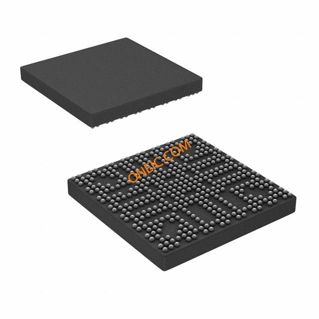
423-FCBGA-CUS
Image Preview