MM74HCT08MTC
Quad 2-input AND gate ICs in 14-pin TSSOP for logic applications
Manufacturer: ['fairchild', 'rochester', 'onsemi', 'freescale']
series introduction
# MM74HCT08MTC Product Series Introduction
## 1. Overview
The MM74HCT08MTC belongs to the 74HCT series of integrated circuits, which are widely recognized in the electronics industry for their high - performance and reliability. This specific product is a quad 2 - input AND gate, designed to perform logical AND operations on digital signals. It combines the advantages of high - speed operation and compatibility with both TTL (Transistor - Transistor Logic) and CMOS (Complementary Metal - Oxide - Semiconductor) logic levels, making it a versatile choice for a variety of digital circuit applications.
## 2. Key Features
### 2.1 Logic Function
As a quad 2 - input AND gate, the MM74HCT08MTC contains four independent AND gates within a single package. Each AND gate has two input pins and one output pin. The output of an AND gate is high (logic 1) only when both of its inputs are high. Mathematically, if we denote the two inputs as A and B and the output as Y, then \(Y = A\cdot B\). This basic logic function is fundamental in digital circuit design for tasks such as signal masking, data encoding, and control signal generation.
### 2.2 High - Speed Operation
The HCT (High - Speed CMOS TTL - compatible) technology used in the MM74HCT08MTC enables it to achieve relatively fast propagation delays. Propagation delay is the time it takes for a change in the input signal to result in a corresponding change in the output signal. With low propagation delays, this device can handle high - frequency digital signals, making it suitable for applications where fast data processing is required, such as in high - speed communication systems and microprocessor - based circuits.
### 2.3 Compatibility
One of the significant advantages of the MM74HCT08MTC is its compatibility with both TTL and CMOS logic levels. TTL logic has been a long - standing standard in digital electronics, and many legacy systems still use TTL - level signals. CMOS logic, on the other hand, offers low power consumption and high noise immunity. The MM74HCT08MTC can interface seamlessly between TTL and CMOS circuits, allowing for easy integration into existing systems or the design of hybrid - logic circuits.
### 2.4 Low Power Consumption
CMOS technology inherently consumes less power compared to some other logic families. The MM74HCT08MTC takes advantage of this characteristic, making it an energy - efficient choice for battery - powered devices or applications where power consumption is a critical concern. In standby mode, the power consumption is extremely low, which helps to extend the battery life of portable electronics.
### 2.5 High Noise Immunity
The MM74HCT08MTC has good noise immunity, which means it can tolerate a certain amount of electrical noise on its input signals without producing incorrect output results. This is crucial in real - world environments where electrical interference is common, such as in industrial settings or near high - power electrical equipment. The high noise immunity ensures the reliability and stability of the digital circuits in which the device is used.
## 3. Package and Pin Configuration
### 3.1 Package Type
The MM74HCT08MTC is typically available in a small - outline integrated circuit (SOIC) package. The SOIC package is a surface - mount package that offers several advantages, including a small footprint, which is beneficial for printed circuit board (PCB) design, especially in applications where space is limited. It also provides good thermal performance and is suitable for automated assembly processes, which helps to reduce manufacturing costs.
### 3.2 Pin Configuration
The device has a total of 14 pins.
Images for reference
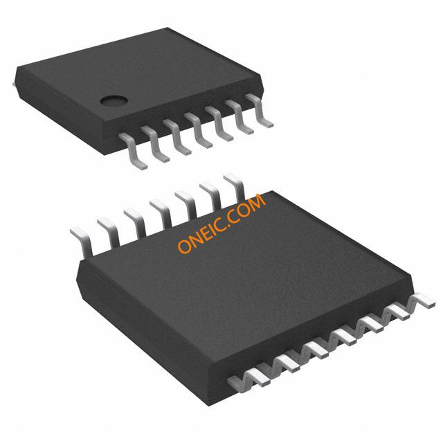
14-TSSOP

Image Preview
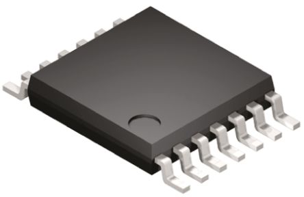
Image Preview