MC14021BDG
8-bit CMOS shift registers in 16-pin SOIC for serial/parallel data conversion
Manufacturer: ['rochester', 'onsemi']
series introduction
# Introduction to the MC14021BDG Product Series
## 1. Overview
The MC14021BDG belongs to a well - established family of integrated circuits. It is a high - performance, 8 - stage static shift register designed by ON Semiconductor. This product series is widely used in various electronic applications due to its reliable performance, ease of use, and compatibility with different circuit designs.
## 2. Key Features
### 2.1 Logic Functionality
- **Shift Register Operation**: The MC14021BDG operates as an 8 - stage static shift register. It can store and shift data bits in a sequential manner. This functionality is crucial in applications where data needs to be transferred or processed in a step - by - step fashion. For example, in serial - to - parallel data conversion, the shift register can receive serial data and then present it in parallel form for further processing.
- **Two Clock Inputs**: It features two clock inputs, namely the positive - edge - triggered clock (CP) and the negative - edge - triggered clock (CE). This dual - clock design provides flexibility in controlling the shifting operation. Designers can choose the appropriate clock edge based on the requirements of their specific application, allowing for better synchronization with other components in the circuit.
### 2.2 Electrical Characteristics
- **Wide Supply Voltage Range**: The MC14021BDG can operate over a wide supply voltage range, typically from 3V to 18V. This wide range makes it suitable for use in different power supply environments, whether it is a low - voltage battery - powered device or a higher - voltage industrial application.
- **Low Power Consumption**: With its CMOS technology, the MC14021BDG consumes relatively low power. This is especially important in battery - operated devices, as it helps to extend the battery life. The low power consumption also reduces heat generation, which can enhance the reliability and longevity of the circuit.
### 2.3 Compatibility
- **TTL/CMOS Compatibility**: The input and output levels of the MC14021BDG are compatible with both TTL (Transistor - Transistor Logic) and CMOS (Complementary Metal - Oxide - Semiconductor) logic families. This compatibility allows it to be easily integrated into existing circuits that use either TTL or CMOS components, providing greater design flexibility.
## 3. Pin Configuration
The MC14021BDG comes in a standard 16 - pin dual - in - line package (DIP) or a surface - mount package (SOIC). The pin configuration is carefully designed to facilitate easy connection to other components in the circuit.
- **Data Input Pins**: There are dedicated pins for serial data input (DS) and parallel data input (P0 - P7). The serial data input is used when data is to be shifted into the register one bit at a time, while the parallel data input allows for the simultaneous loading of all 8 bits into the register.
- **Clock and Control Pins**: The positive - edge - triggered clock (CP), negative - edge - triggered clock (CE), and the parallel load control (PL) pins are provided. The PL pin, when activated, allows the parallel data to be loaded into the register, overriding the normal shifting operation.
- **Output Pins**: The 8 output pins (Q0 - Q7) provide the shifted or loaded data. These outputs can be connected to other components such as microcontrollers, displays, or other logic circuits for further processing.
## 4. Applications
### 4.1 Data Communication
- **Serial - to - Parallel Conversion**: In communication systems where data is transmitted serially, the MC14021BDG can be used to convert the serial data
Images for reference

16 SOIC

Image Preview
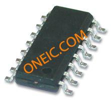
Image Preview