LT1019ACN8-2.5
Precision 2.5V voltage reference ICs in 8-pin PDIP packages
Manufacturer: linear-technology
series introduction
# LT1019ACN8 - 2.5 Product Series Introduction
## 1. Overview
The LT1019ACN8 - 2.5 is a highly reliable and precision voltage reference product series offered by Linear Technology (now part of Analog Devices). Voltage references are crucial components in a wide range of electronic circuits as they provide a stable and accurate voltage output that can be used as a benchmark for other circuit elements. The LT1019ACN8 - 2.5 is specifically designed to meet the demanding requirements of applications where high precision, low noise, and excellent temperature stability are essential.
## 2. Key Features
### 2.1 Precision Output Voltage
The LT1019ACN8 - 2.5 provides a fixed output voltage of 2.5V with a high degree of accuracy. The initial accuracy of the device is typically very tight, ensuring that the output voltage remains close to the nominal 2.5V value right from the start. This precision is vital in applications such as analog - to - digital converters (ADCs), digital - to - analog converters (DACs), and precision measurement circuits, where even small deviations in the reference voltage can lead to significant errors in the overall system performance.
### 2.2 Low Temperature Coefficient
One of the standout features of the LT1019ACN8 - 2.5 is its low temperature coefficient. Temperature changes can have a significant impact on the output voltage of a voltage reference. However, this product series is engineered to minimize the effect of temperature variations. A low temperature coefficient means that the output voltage remains relatively stable over a wide temperature range. This makes the LT1019ACN8 - 2.5 suitable for use in environments where the temperature can fluctuate, such as industrial control systems, automotive electronics, and outdoor monitoring equipment.
### 2.3 Low Noise
In precision applications, noise can be a major source of interference. The LT1019ACN8 - 2.5 is designed to have low output noise, which helps to ensure that the reference voltage is clean and free from unwanted fluctuations. This is particularly important in applications like high - resolution ADCs, where noise in the reference voltage can degrade the signal - to - noise ratio and reduce the overall accuracy of the conversion process.
### 2.4 High Power Supply Rejection Ratio (PSRR)
The power supply rejection ratio is a measure of how well a voltage reference can reject variations in the power supply voltage. The LT1019ACN8 - 2.5 has a high PSRR, which means that it can maintain a stable output voltage even when there are fluctuations in the input power supply. This is beneficial in applications where the power supply may be noisy or subject to voltage spikes, such as in power - hungry electronic systems or in environments with poor power quality.
### 2.5 Small Package Size
The LT1019ACN8 - 2.5 comes in a compact 8 - pin plastic DIP (Dual In - Line Package) or SOIC (Small Outline Integrated Circuit) package. The small package size makes it easy to integrate into printed circuit boards (PCBs) with limited space. This is advantageous in applications where miniaturization is a key requirement, such as in portable electronic devices, handheld test equipment, and wearable technology.
## 3. Applications
### 3.1 Analog - to - Digital and Digital - to - Analog Conversion
In ADCs and DACs, the LT1019ACN8 - 2.5 serves as a stable reference voltage. The high precision and low noise characteristics of the device ensure accurate conversion between analog and digital signals. For example, in a data acquisition system, an ADC uses the reference voltage provided by the
Images for reference
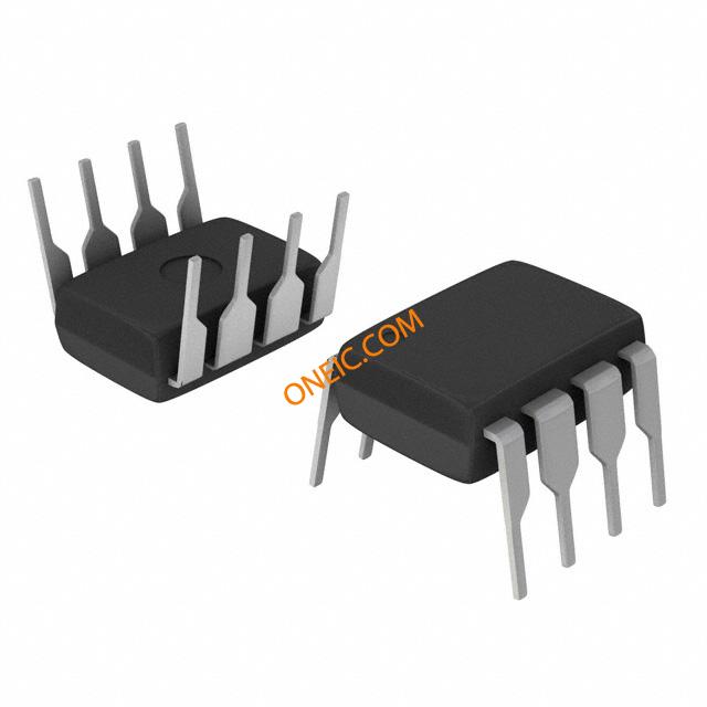
8-DIP
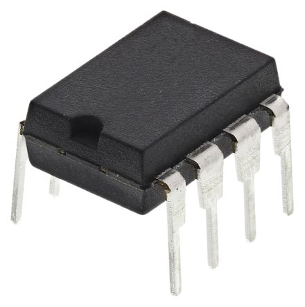
Image Preview
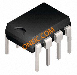
Image Preview