LFXP2-8E-5MN132C
Compact FPGAs with 86 I/O, 1.2V, and 132-pin BGA for versatile applications
Manufacturer: lattice
series introduction
# Introduction to the LFXP2 - 8E - 5MN132C Product Series
## 1. Overview
The LFXP2 - 8E - 5MN132C belongs to a specialized and high - performance product series, typically falling within the realm of programmable logic devices (PLDs). These devices are at the heart of modern electronics, enabling designers to implement custom digital circuits without the need for full - scale custom integrated circuit fabrication. This particular product offers a unique combination of features, performance, and flexibility, making it suitable for a wide range of applications.
## 2. Key Specifications
### 2.1 Logic Capacity
The "8E" in the model number indicates a certain level of logic capacity. It provides a sufficient number of logic elements, such as look - up tables (LUTs) and flip - flops, to implement moderately complex digital designs. These logic elements can be configured to perform various functions, including arithmetic operations, state machine implementations, and data routing.
### 2.2 Speed Grade
The "5" represents the speed grade of the device. A lower speed grade number generally implies a higher - speed device. This means that the LFXP2 - 8E - 5MN132C can operate at relatively high clock frequencies, allowing for fast data processing and quick response times in time - critical applications. It can handle high - speed data streams and perform operations within tight timing constraints.
### 2.3 Package Type
The "MN132" refers to the package type of the device. The 132 - pin package provides a specific physical form factor and a set of input/output (I/O) connections. This package is designed to be compatible with standard printed circuit board (PCB) manufacturing processes, making it easy to integrate into existing or new circuit designs. The I/O pins can be used to interface with other components in the system, such as microcontrollers, memory devices, and sensors.
### 2.4 Temperature Grade
The "C" typically indicates the commercial temperature grade. This means that the device is designed to operate reliably within a temperature range suitable for most commercial applications, usually from 0°C to 70°C. This temperature range ensures stable performance in normal office, industrial, and consumer electronics environments.
## 3. Features
### 3.1 Programmability
One of the most significant features of the LFXP2 - 8E - 5MN132C is its programmability. Designers can use hardware description languages (HDLs) such as VHDL or Verilog to describe the desired digital circuit behavior. The device can then be programmed using a programming tool, which configures the internal logic elements and interconnections according to the design specifications. This allows for rapid prototyping and easy design modifications, reducing development time and cost.
### 3.2 Embedded Memory
The product series may include embedded memory blocks, such as random - access memory (RAM). These memory blocks can be used to store data temporarily during the operation of the digital circuit. For example, they can be used to buffer data in a data acquisition system or to store intermediate results in a digital signal processing application.
### 3.3 I/O Flexibility
The 132 - pin package offers a wide range of I/O options. The I/O pins can be configured to support different voltage levels and signaling standards, such as TTL (Transistor - Transistor Logic), CMOS (Complementary Metal - Oxide - Semiconductor), and LVDS (Low - Voltage Differential Signaling). This flexibility allows the device to interface with a variety of external components and systems, making it suitable for diverse applications.
### 3.4 Low Power Consumption
In today's energy - conscious world, low power consumption is a crucial feature. The LFXP2 -
Images for reference
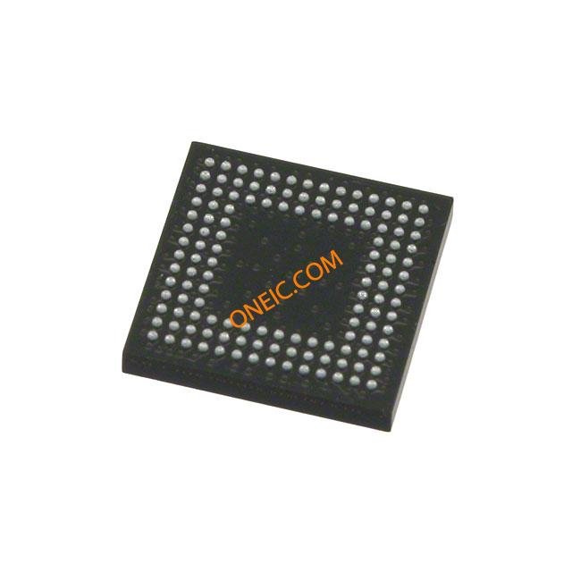
132CSBGA
Image Preview