JANTX2N3440
General-purpose NPN bipolar junction transistors for various electronic circuits
Manufacturer: microsemi
series introduction
# JANTX2N3440 Product Series Introduction
## 1. Overview
The JANTX2N3440 product series is a highly specialized and reliable line of semiconductor devices that play a crucial role in a wide range of electronic applications. These devices are designed to meet the stringent requirements of military and aerospace industries, where high performance, durability, and precision are of utmost importance.
## 2. Device Type and Function
The JANTX2N3440 is a type of N - channel junction field - effect transistor (JFET). JFETs are a class of field - effect transistors that operate based on the control of current flow through a semiconductor channel by an electric field. In the case of the N - channel JFET, the majority carriers are electrons.
### Key Functions
- **Amplification**: It can amplify weak electrical signals. By controlling the input voltage at the gate terminal, the JFET can modulate the current flowing between the source and the drain terminals, resulting in an amplified output signal. This makes it suitable for use in audio amplifiers, radio frequency (RF) amplifiers, and other signal - processing circuits.
- **Switching**: The JANTX2N3440 can also be used as a switch. When a certain voltage is applied to the gate, the channel between the source and drain can be either opened or closed, allowing or blocking the flow of current. This switching function is essential in digital circuits, power management systems, and other applications where the control of electrical current is required.
## 3. Electrical Characteristics
### Voltage Ratings
- **Drain - Source Voltage (VDS)**: The JANTX2N3440 is designed to handle a specific maximum drain - source voltage. This rating determines the maximum voltage that can be applied across the drain and source terminals without causing damage to the device. For the JANTX2N3440, the VDS rating is carefully specified to ensure reliable operation in high - voltage environments.
- **Gate - Source Voltage (VGS)**: The gate - source voltage is used to control the conductivity of the channel. The device has a defined range of VGS values within which it operates optimally. By varying the VGS, the user can adjust the drain current (ID) flowing through the device.
### Current Ratings
- **Drain Current (ID)**: This is the current that flows between the drain and the source terminals. The JANTX2N3440 has a specified maximum drain current rating, which indicates the maximum amount of current the device can handle continuously without overheating or suffering damage.
- **Gate Current (IG)**: The gate current is typically very small in a JFET, as the gate - channel junction is reverse - biased. The low gate current characteristic of the JANTX2N3440 makes it suitable for applications where low power consumption and high input impedance are required.
### Transconductance (gm)
Transconductance is a measure of how effectively the gate voltage controls the drain current. A higher transconductance value means that a small change in the gate voltage can result in a relatively large change in the drain current. The JANTX2N3440 has a well - defined transconductance characteristic, which is important for applications such as amplifier design, where efficient signal amplification is desired.
## 4. Package and Physical Characteristics
### Package Type
The JANTX2N3440 is available in a specific package type that is designed to provide mechanical protection and electrical connection to the device. Common package types for this series may include through - hole packages, which are suitable for traditional printed circuit board (PCB) assembly methods. The package is designed to ensure good heat dissipation, as the device may generate heat during operation.
### Dimensions
Images for reference
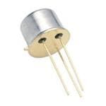
Image Preview