HCF4094BE
8-stage shift register ICs for serial to parallel data conversion
Manufacturer: stm
series introduction
# HCF4094BE Product Series Introduction
## 1. Overview
The HCF4094BE is a part of the 4000 series of CMOS integrated circuits. It is a 8 - stage shift register with a storage register and 3 - state outputs. This device combines the functionality of a shift register and a storage register, making it highly versatile for a wide range of digital applications. It is designed to operate over a wide supply - voltage range, which enhances its compatibility with different power sources and systems.
## 2. Key Features
### 2.1 Shift Register Functionality
- **8 - Stage Structure**: The HCF4094BE has eight stages, which means it can store and shift up to eight bits of data. This is useful for applications such as serial - to - parallel data conversion. For example, in a communication system where data is received serially, the shift register can collect the incoming bits one by one and then present them in parallel form for further processing.
- **Serial Input**: It has a serial data input (DS), which allows data to be entered into the shift register bit by bit. This is a common method of data transfer in many digital systems, especially when dealing with long - distance communication where sending data serially is more efficient.
### 2.2 Storage Register
- **Data Latching**: The device includes a storage register. The data stored in the shift register can be transferred to the storage register using the strobe input (STROBE). This feature is beneficial in applications where the data needs to be held stable for a certain period. For instance, in a display system, the data can be shifted into the shift register and then latched into the storage register to ensure a stable display.
### 2.3 3 - State Outputs
- **Output Control**: The 3 - state outputs (Q0 - Q7) can be put into a high - impedance state using the output enable input (OE). This is extremely useful in bus - based systems. When the outputs are in the high - impedance state, they do not load the bus, allowing other devices to communicate on the same bus without interference.
### 2.4 Wide Supply Voltage Range
- **Flexibility**: The HCF4094BE can operate with a supply voltage (VDD - VSS) ranging from 3V to 18V. This wide range makes it suitable for use in various systems, from low - power battery - operated devices to high - voltage industrial applications.
### 2.5 Low Power Consumption
- **Energy Efficiency**: As a CMOS device, it consumes very low power, especially in standby or idle states. This is an important feature for battery - powered devices, as it helps to extend the battery life.
## 3. Pin Configuration
### 3.1 Input Pins
- **DS (Serial Data Input)**: This pin is used to input data serially into the shift register. The data is shifted into the first stage of the shift register on the rising edge of the clock signal.
- **CP (Clock Pulse Input)**: The clock signal applied to this pin controls the shifting of data through the shift register. Each rising edge of the clock causes the data in the shift register to move one stage forward.
- **STROBE**: When a high - level signal is applied to the strobe input, the data in the shift register is transferred to the storage register.
- **OE (Output Enable)**: A low - level signal on this pin enables the 3 - state outputs, allowing the data stored in the storage register to be presented on the output pins. A high - level signal puts the outputs in a high - impedance state.
### 3.2 Output Pins
- **Q0 - Q7**:
Images for reference
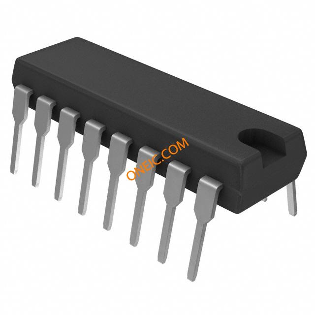
16-DIP SOT38-1
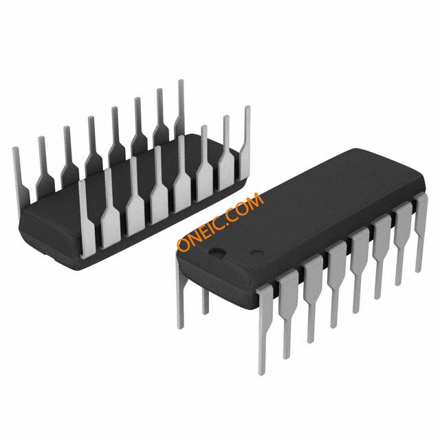
16-Dip
Image Preview