EP4CE55F23I7N
Field programmable gate arrays with 324 I/O interfaces
Manufacturer: altera
series introduction
# Introduction to the EP4CE55F23I7N Product Series
## 1. Overview
The EP4CE55F23I7N belongs to the Cyclone IV E family of Field - Programmable Gate Arrays (FPGAs) developed by Altera (now Intel). FPGAs are integrated circuits that can be programmed and reprogrammed by the user after manufacturing, offering a high degree of flexibility for a wide range of applications. The EP4CE55F23I7N is designed to provide a cost - effective and high - performance solution for various digital design tasks.
## 2. Key Features
### 2.1 Logic Resources
- **Logic Elements (LEs)**: The EP4CE55F23I7N is equipped with approximately 55,000 logic elements. LEs are the basic building blocks of an FPGA, used to implement combinational and sequential logic functions. This large number of LEs allows designers to implement complex digital circuits, such as state machines, arithmetic units, and data processing pipelines.
- **Adaptive Logic Modules (ALMs)**: The FPGA uses ALMs, which are more advanced than traditional LEs. ALMs can be configured to perform different logic functions efficiently, reducing the overall resource usage and improving the performance of the design.
### 2.2 Memory Resources
- **Embedded Memory**: It has a significant amount of embedded memory in the form of M9K memory blocks. These memory blocks can be configured as single - port, dual - port, or true dual - port RAM, as well as ROM or FIFO buffers. The embedded memory is useful for storing data, such as look - up tables, intermediate results in digital signal processing, and configuration data.
- **Total Memory Capacity**: The total embedded memory capacity of the EP4CE55F23I7N is sufficient to handle medium - sized data storage requirements in various applications.
### 2.3 Digital Signal Processing (DSP) Blocks
- **DSP Slices**: The FPGA contains multiple DSP slices. These slices are optimized for performing high - speed arithmetic operations, such as multiplication, addition, and accumulation. They are particularly useful in applications such as digital filtering, image processing, and communication systems.
- **High - Speed Processing**: The DSP blocks can operate at high clock frequencies, enabling real - time processing of data streams. This makes the EP4CE55F23I7N suitable for applications that require fast signal processing, such as wireless communication base stations and video processing systems.
### 2.4 I/O Resources
- **I/O Pins**: It offers a large number of general - purpose I/O (GPIO) pins. These pins can be configured to support different I/O standards, such as LVCMOS, LVDS, and SSTL. This flexibility allows the FPGA to interface with a wide variety of external devices, including microcontrollers, sensors, and memory chips.
- **High - Speed I/O**: Some of the I/O pins support high - speed data transfer rates, which is essential for applications that require high - bandwidth communication, such as Ethernet interfaces and high - speed serial links.
### 2.5 Power Efficiency
- **Low - Power Design**: The Cyclone IV E family, including the EP4CE55F23I7N, is designed with power - saving features. It uses a low - power process technology and has power management options that allow designers to optimize the power consumption of their designs. This is particularly important for battery - powered devices and applications where power efficiency is a critical factor.
## 3. Package and Pinout
- **Package Type**: The EP4CE55F23I7N comes in a 23 - mm FineLine Ball Grid Array (FBGA
Images for reference
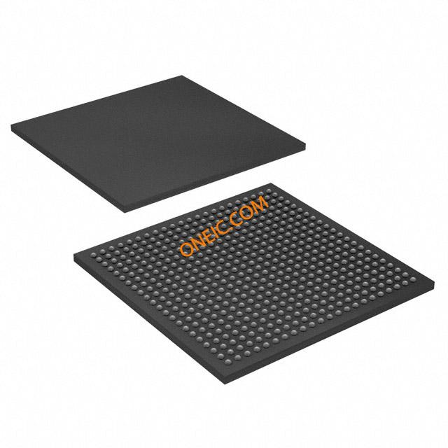
484-FBGA
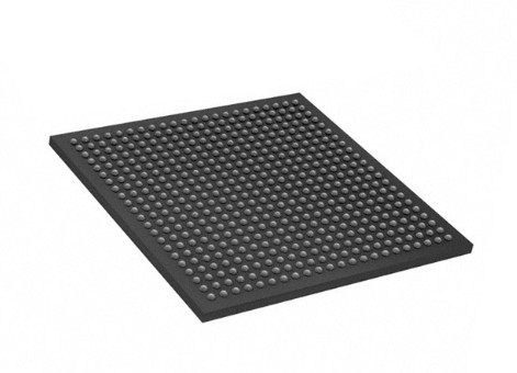
Image Preview
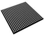
Image Preview