EP3C40F484C6
Cyclone III FPGAs with multiple I/O options and configurable logic blocks
Manufacturer: altera
series introduction
# Introduction to the EP3C40F484C6 Product Series
## 1. Overview
The EP3C40F484C6 belongs to the Cyclone III family of Field - Programmable Gate Arrays (FPGAs) developed by Altera (now Intel). FPGAs are integrated circuits that can be programmed and reprogrammed by the user after manufacturing, offering a high degree of flexibility for a wide range of applications. The EP3C40F484C6 is designed to provide a balance between performance, cost, and power consumption, making it suitable for various industrial, consumer, and communication applications.
## 2. Key Features
### 2.1 Logic Resources
- **Logic Elements (LEs)**: The EP3C40F484C6 is equipped with approximately 40,000 logic elements. LEs are the basic building blocks of an FPGA, used to implement combinational and sequential logic functions. This large number of LEs allows designers to implement complex digital circuits, such as state machines, arithmetic units, and control logic.
- **Configurable Logic Blocks (CLBs)**: These are groups of LEs that can be configured to perform specific functions. The CLBs in the EP3C40F484C6 provide a high - level of flexibility, enabling designers to optimize the use of logic resources for different applications.
### 2.2 Memory Resources
- **Embedded Memory**: It has a significant amount of embedded memory in the form of Block RAM (BRAM). The BRAM can be used for various purposes, such as data buffering, FIFO (First - In - First - Out) queues, and lookup tables. This on - chip memory reduces the need for external memory components, simplifying the system design and improving performance.
- **Distributed Memory**: In addition to BRAM, the FPGA also has distributed memory, which is used for smaller - scale memory requirements. Distributed memory is integrated within the logic elements, providing a convenient way to store small amounts of data close to the logic that uses it.
### 2.3 I/O Resources
- **I/O Pins**: The EP3C40F484C6 comes with 484 I/O pins. These pins can be configured to support a wide range of I/O standards, including LVCMOS (Low - Voltage Complementary Metal - Oxide - Semiconductor), LVTTL (Low - Voltage Transistor - Transistor Logic), and differential signaling standards such as LVDS (Low - Voltage Differential Signaling). This flexibility allows the FPGA to interface with different types of external devices, such as microcontrollers, sensors, and communication interfaces.
- **I/O Banks**: The I/O pins are organized into multiple I/O banks, each with its own power supply and configuration options. This allows for independent control of different groups of I/O pins, enabling designers to optimize the power consumption and signal integrity of the system.
### 2.4 Clock Management
- **Phase - Locked Loops (PLLs)**: The FPGA includes multiple PLLs, which are used for clock generation and synchronization. PLLs can generate multiple clock signals with different frequencies and phases from a single input clock. This is essential for applications that require precise timing, such as high - speed data communication and digital signal processing.
- **Delay - Locked Loops (DLLs)**: DLLs are used to compensate for clock skew and delay in the system. They ensure that the clock signals arrive at different parts of the FPGA at the same time, improving the overall performance and reliability of the circuit.
### 2.5 Power Management
- **Low - Power Operation**: The EP3C40F484C6 is designed to operate with low power
Images for reference
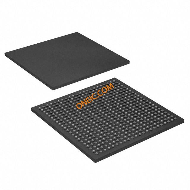
484-FBGA

Image Preview
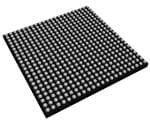
Image Preview