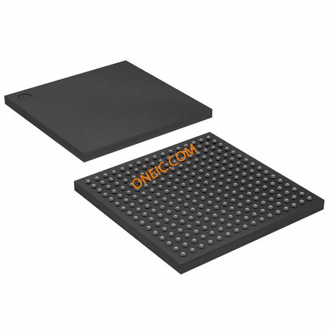
EP3C25U256C7N
Field programmable gate arrays with 156 I/O interfaces
Manufacturer: altera
series introduction
# Introduction to the EP3C25U256C7N Product Series
## 1. Overview
The EP3C25U256C7N belongs to a specific family of Field - Programmable Gate Arrays (FPGAs) offered by Altera (now Intel). FPGAs are integrated circuits that can be programmed and reprogrammed by the user after manufacturing, providing a high degree of flexibility for a wide range of applications. The EP3C25U256C7N is designed to meet the needs of various industries, including telecommunications, industrial automation, automotive, and consumer electronics.
## 2. Key Features
### 2.1 Logic Capacity
- The "25" in the part number indicates a significant logic capacity. It has approximately 25,000 logic elements (LEs). These LEs are the basic building blocks of the FPGA, capable of implementing combinational and sequential logic functions. This allows designers to create complex digital circuits, such as microprocessors, digital signal processing (DSP) algorithms, and custom control logic.
### 2.2 Package Type
- The "U256" refers to the package type. It comes in a 256 - pin package. The package provides the physical interface between the FPGA die and the printed circuit board (PCB). The 256 - pin package offers a sufficient number of input/output (I/O) pins, which are crucial for connecting the FPGA to external components such as memory chips, sensors, and communication interfaces.
### 2.3 Speed Grade
- The "C7" represents the speed grade. A lower speed grade number generally indicates better performance in terms of maximum operating frequency and propagation delay. The C7 speed grade ensures that the EP3C25U256C7N can operate at relatively high clock frequencies, enabling it to handle high - speed data processing tasks.
### 2.4 Configuration
- The "N" in the part number may refer to a specific configuration option. It could be related to the type of configuration memory or the way the FPGA is initialized. The FPGA can be configured using different methods, such as in - system programming (ISP) or external configuration devices.
## 3. Performance Characteristics
### 3.1 Clock Frequency
- Thanks to its C7 speed grade, the EP3C25U256C7N can support high - speed clock signals. It can operate at clock frequencies that are suitable for many real - time applications, such as high - speed data acquisition and processing systems. This high - speed operation is essential for applications that require fast data transfer and processing, like video and audio processing.
### 3.2 Power Consumption
- FPGAs are known for their relatively low power consumption compared to other programmable devices. The EP3C25U256C7N is designed with power - saving features, such as power - down modes and dynamic power management. This makes it suitable for battery - powered devices or applications where power efficiency is a critical factor.
### 3.3 Signal Integrity
- The FPGA has built - in features to ensure good signal integrity. It can handle high - speed signals with minimal noise and interference. This is important for reliable communication between the FPGA and external components, especially in high - speed data transfer applications.
## 4. Application Areas
### 4.1 Telecommunications
- In telecommunications systems, the EP3C25U256C7N can be used for tasks such as protocol conversion, signal processing, and network management. It can implement custom communication protocols and handle high - speed data streams, making it suitable for use in routers, switches, and base stations.
### 4.2 Industrial Automation
- For industrial automation applications
Images for reference
DS-256BGA205-2_0
Image Preview