EP3C16M164I7N
Compact, high-performance FPGAs for versatile digital circuit applications
Manufacturer: altera
series introduction
# Introduction to the EP3C16M164I7N Product Series
## 1. Overview
The EP3C16M164I7N belongs to a specific family of Field - Programmable Gate Arrays (FPGAs) developed by Altera (now part of Intel). FPGAs are integrated circuits that can be programmed and reprogrammed by the user after manufacturing, offering a high degree of flexibility for a wide range of applications. The EP3C16M164I7N is designed to provide a balance between performance, cost, and power consumption, making it suitable for various industrial, consumer, and communication applications.
## 2. Key Features
### 2.1 Logic Resources
- **Logic Elements (LEs)**: The EP3C16M164I7N is equipped with a significant number of logic elements. These LEs are the basic building blocks of the FPGA, capable of implementing combinational and sequential logic functions. With a sufficient number of LEs, it can handle complex digital designs, such as state machines, arithmetic circuits, and data processing units.
- **Configurable Logic Blocks (CLBs)**: The FPGA is organized into CLBs, which group multiple LEs together along with associated routing resources. This modular design allows for efficient implementation of larger logic functions and simplifies the design process.
### 2.2 Memory
- **On - Chip Memory**: It has on - chip memory resources, including embedded memory blocks. These memory blocks can be used for storing data, such as look - up tables, buffers, and small - scale data caches. The on - chip memory provides fast access times, which is crucial for applications that require high - speed data processing.
- **Memory Configuration**: The memory can be configured in different ways, such as single - port RAM, dual - port RAM, or ROM, depending on the specific requirements of the application. This flexibility enables designers to optimize the use of memory resources for their particular designs.
### 2.3 I/O Capabilities
- **Multiple I/O Standards**: The EP3C16M164I7N supports a wide range of I/O standards, including LVTTL, LVCMOS, and differential signaling standards like LVDS. This allows it to interface with various external devices, such as microcontrollers, sensors, and communication interfaces.
- **I/O Pins**: It has a sufficient number of I/O pins, which can be used for input and output operations. The I/O pins can be configured as general - purpose I/O (GPIO) or dedicated to specific functions, providing flexibility in system design.
### 2.4 Power Management
- **Low - Power Operation**: The FPGA is designed to operate with relatively low power consumption, making it suitable for battery - powered devices or applications where power efficiency is a critical factor. It incorporates power - saving features, such as dynamic power management and power - down modes, to reduce power consumption during idle or low - activity periods.
- **Power Supply Options**: It supports a wide range of power supply voltages, allowing for easy integration into different power systems. This flexibility in power supply options simplifies the design process and reduces the need for complex power management circuits.
### 2.5 Clock Management
- **PLLs and DLLs**: The EP3C16M164I7N includes Phase - Locked Loops (PLLs) and Delay - Locked Loops (DLLs). PLLs are used for frequency synthesis, clock multiplication, and clock phase adjustment, while DLLs are used for clock delay compensation. These clock management circuits ensure stable and accurate clock signals throughout the FPGA, which is essential for reliable operation of digital circuits.
- **Multiple Clock Domains**: It can support multiple clock domains, allowing different parts
Images for reference
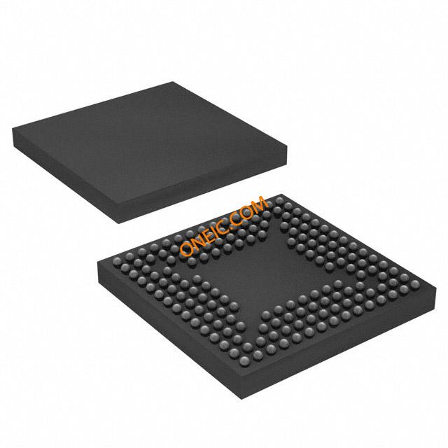
164-MBGA
Image Preview

Image Preview