EP3C120F484I7
Field programmable gate arrays with 283 I/O for versatile electronic designs
Manufacturer: altera
series introduction
# Introduction to the EP3C120F484I7 Product Series
## 1. Overview
The EP3C120F484I7 belongs to the Cyclone III family of Field - Programmable Gate Arrays (FPGAs) developed by Altera (now Intel). FPGAs are semiconductor devices that can be programmed and reprogrammed by the user after manufacturing, offering a high degree of flexibility for a wide range of applications. The EP3C120F484I7 is specifically designed to provide a balance between performance, cost, and power consumption, making it suitable for various industrial, communication, and consumer electronics applications.
## 2. Key Features
### Logic Resources
- **Logic Elements (LEs)**: The EP3C120F484I7 is equipped with approximately 120,000 logic elements. These LEs are the basic building blocks of the FPGA, capable of implementing combinational and sequential logic functions. They can be used to create complex digital circuits such as arithmetic units, state machines, and control logic.
- **Embedded Memory**: It has a significant amount of embedded memory, including embedded Multi - Port Memories (eMPMs) and embedded RAM blocks. This memory can be used for data storage, buffering, and implementing functions like FIFO (First - In - First - Out) queues and lookup tables. The availability of on - chip memory reduces the need for external memory components, simplifying the overall system design and potentially reducing costs.
### I/O Capabilities
- **I/O Pins**: With 484 I/O pins, the EP3C120F484I7 offers a rich set of input/output interfaces. These pins can be configured to support a variety of standard I/O protocols, such as LVDS (Low - Voltage Differential Signaling), SSTL (Stub Series Terminated Logic), and LVCMOS (Low - Voltage Complementary Metal - Oxide - Semiconductor). This flexibility allows the FPGA to interface with different types of external devices, including microcontrollers, sensors, and communication modules.
- **I/O Standards Support**: The support for multiple I/O standards enables the FPGA to be used in diverse applications. For example, LVDS is commonly used for high - speed data transmission, making it suitable for applications such as video processing and high - speed communication links. SSTL is often used in memory interfaces, while LVCMOS is a general - purpose I/O standard that can be used for interfacing with a wide range of digital devices.
### Performance
- **Clock Speed**: The EP3C120F484I7 can operate at relatively high clock speeds, allowing it to handle high - frequency digital signals. This high - speed operation is crucial for applications that require real - time processing, such as signal processing and communication systems.
- **Signal Propagation Delay**: The FPGA has low signal propagation delays, which means that the time taken for a signal to travel through the logic circuits is minimized. This results in faster overall system response times and better performance in time - critical applications.
### Power Consumption
- **Low - Power Design**: Altera has designed the Cyclone III family, including the EP3C120F484I7, with power efficiency in mind. The FPGA uses advanced semiconductor manufacturing processes and power management techniques to reduce power consumption. This is particularly important for battery - powered devices and applications where energy efficiency is a key concern.
## 3. Package and Thermal Considerations
### Package Type
The "F484" in the part number indicates the package type. In this case, it is a Fine - pitch Ball Grid Array (FBGA) package with 484 pins. The FBGA package offers several advantages, including
Images for reference
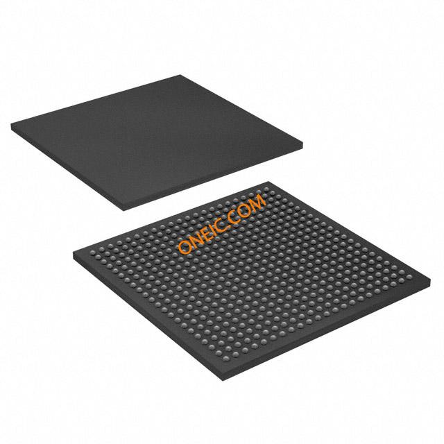
484-FBGA
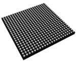
Image Preview