EP2S180F1508I4N
High-performance FPGA with extensive I/O and logic array capabilities
Manufacturer: altera
series introduction
# Introduction to the EP2S180F1508I4N Product Series
## 1. Overview
The EP2S180F1508I4N belongs to a high - performance field - programmable gate array (FPGA) product series. FPGAs are semiconductor devices that offer a high degree of flexibility, allowing users to configure the hardware functionality according to their specific application requirements. The EP2S180F1508I4N is designed to meet the complex needs of various industries, including telecommunications, industrial automation, automotive, and high - performance computing.
## 2. Key Features
### 2.1 Logic Capacity
With a substantial logic element (LE) count, the EP2S180F1508I4N provides a large amount of programmable logic resources. This high logic capacity enables the implementation of complex digital circuits, such as multi - core processors, digital signal processing (DSP) algorithms, and custom state machines. It can handle large - scale design projects with ease, allowing designers to integrate multiple functions onto a single chip.
### 2.2 Memory Resources
The product series is equipped with a significant amount of on - chip memory. This includes both random - access memory (RAM) and embedded memory blocks. The on - chip RAM can be used for data storage and buffering during the operation of the FPGA. The embedded memory blocks are optimized for specific applications, such as storing lookup tables, coefficient values for DSP algorithms, and configuration data. The availability of ample memory resources reduces the need for external memory components, thereby simplifying the overall system design and reducing cost.
### 2.3 High - Speed I/O
The EP2S180F1508I4N features a wide range of high - speed input/output (I/O) interfaces. These interfaces support various communication standards, such as LVDS (Low - Voltage Differential Signaling), PCI Express, and Ethernet. The high - speed I/O capabilities enable the FPGA to communicate with other devices at high data rates, making it suitable for applications that require fast data transfer, such as high - speed data acquisition systems and network routers.
### 2.4 DSP Blocks
Integrated DSP blocks are a notable feature of this product series. These blocks are optimized for performing digital signal processing tasks, such as filtering, Fourier transforms, and matrix multiplications. The DSP blocks can operate at high clock frequencies, providing high - performance DSP capabilities within the FPGA. This is particularly useful in applications such as audio and video processing, wireless communication, and radar systems.
### 2.5 Power Efficiency
Despite its high performance, the EP2S180F1508I4N is designed with power efficiency in mind. It incorporates advanced power management techniques, such as dynamic power scaling and power gating. These techniques allow the FPGA to adjust its power consumption based on the workload, reducing overall power consumption and heat generation. This is crucial for applications where power consumption is a critical factor, such as battery - powered devices and data centers.
## 3. Package and Pinout
The EP2S180F1508I4N comes in a specific package with a 1508 - pin configuration. The package is designed to provide good electrical performance, mechanical stability, and thermal dissipation. The pinout of the device is carefully designed to ensure easy connection to external components and printed circuit boards (PCBs). The pins are grouped according to their functions, such as power pins, I/O pins, and configuration pins, making it easier for designers to route the traces on the PCB.
## 4. Configuration and Programming
The FPGA can be configured and programmed using various methods. It supports both in - system programming (ISP) and off - system programming. In - system programming
Images for reference
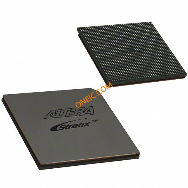
1508-FBGA STRATIX
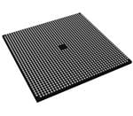
Image Preview