EP2C35F484C8N
Cyclone II series FPGAs with high I/O and logic elements
Manufacturer: altera
series introduction
# Introduction to the EP2C35F484C8N Product Series
## 1. Overview
The EP2C35F484C8N belongs to a high - performance field - programmable gate array (FPGA) product series. FPGAs are semiconductor devices that offer a high degree of flexibility, allowing users to configure the hardware functionality according to their specific application requirements. The EP2C35F484C8N is designed to meet the diverse needs of various industries, including telecommunications, industrial automation, automotive, and consumer electronics.
## 2. Key Features
### 2.1 Logic Capacity
- The "35" in the part number EP2C35F484C8N indicates a significant logic capacity. It provides approximately 35,000 logic elements (LEs). These LEs are the basic building blocks of the FPGA, which can be used to implement a wide range of digital circuits, such as combinational logic, sequential logic, and state machines. This large logic capacity enables the implementation of complex algorithms and systems on a single chip.
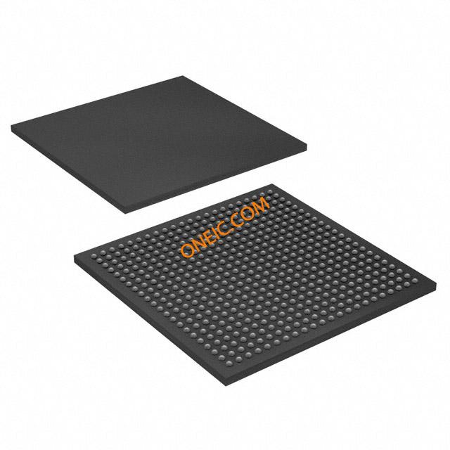
### 2.2 Package Type
- The "F484" represents the package type. It comes in a 484 - pin Fine - pitch Ball Grid Array (FBGA) package. The FBGA package offers several advantages. Firstly, it provides a large number of input/output (I/O) pins, which is crucial for interfacing with external components. Secondly, the fine - pitch design allows for a more compact form factor, making it suitable for applications where space is limited.
### 2.3 Speed Grade
- The "C8" indicates the speed grade of the FPGA. A lower speed grade number generally means better performance in terms of propagation delay and clock frequency. The C8 speed grade ensures that the EP2C35F484C8N can operate at relatively high clock frequencies, enabling fast data processing and real - time operation.
### 2.4 Configuration
- The EP2C35F484C8N uses a SRAM - based configuration technology. This means that the FPGA's configuration data is stored in static random - access memory (SRAM). One of the advantages of SRAM - based FPGAs is their reconfigurability. Users can easily change the functionality of the FPGA by reprogramming the SRAM with new configuration data. This makes the EP2C35F484C8N suitable for prototyping and applications where design changes are frequent.
### 2.5 Embedded Memory
- It is equipped with a certain amount of embedded memory, which can be used for data storage and buffering. The embedded memory can be configured as dual - port RAM, single - port RAM, or ROM, depending on the application requirements. This on - chip memory reduces the need for external memory components, simplifying the system design and reducing the overall cost.
### 2.6 Digital Signal Processing (DSP) Blocks
- The EP2C35F484C8N contains dedicated DSP blocks. These blocks are optimized for performing digital signal processing operations, such as multiplication, addition, and filtering. They can be used to implement complex DSP algorithms, such as fast Fourier transforms (FFTs), digital filters, and audio/video processing algorithms. The presence of DSP blocks significantly enhances the FPGA's ability to handle high - speed signal processing tasks.
## 3. Applications
### 3.1 Telecommunications
- In telecommunications systems, the EP2C35F484C8N can be used for baseband processing, protocol conversion, and signal demodulation. Its high logic capacity and fast processing speed make it suitable for handling the large amounts of data and complex algorithms involved in modern communication systems,
Images for reference
484-FBGA

Image Preview

Image Preview