EP2C35F484C6N
Cyclone II series FPGAs with 322 I/O in 484-pin FBGA package
Manufacturer: altera
series introduction
# Introduction to the EP2C35F484C6N Product Series
## 1. Overview
The EP2C35F484C6N belongs to a highly regarded product series in the field of programmable logic devices (PLDs). Specifically, it is a member of the Cyclone II family of Field - Programmable Gate Arrays (FPGAs) developed by Altera (now Intel). These FPGAs are designed to offer a cost - effective and high - performance solution for a wide range of applications, from consumer electronics to industrial control systems.
## 2. Key Features
### 2.1 Logic Capacity
- The "35" in the EP2C35F484C6N model number indicates its logic element (LE) count. With approximately 35,000 logic elements, it provides a substantial amount of programmable logic resources. This allows designers to implement complex digital circuits, such as state machines, arithmetic units, and data processing algorithms, all within a single device.
- The large logic capacity also enables the integration of multiple functions on a single FPGA, reducing the need for multiple discrete components and simplifying the overall system design.
### 2.2 Package Type
- The "F484" refers to the package type. It comes in a 484 - pin Fine - pitch Ball Grid Array (FBGA) package. This package offers several advantages. Firstly, the fine - pitch design allows for a high - density interconnection, enabling a large number of input/output (I/O) pins to be available on a relatively small footprint.
- The BGA package also provides good thermal performance as the balls on the bottom of the package act as heat transfer paths, helping to dissipate the heat generated during operation.
### 2.3 Speed Grade
- The "C6" represents the speed grade of the FPGA. A lower speed grade number generally indicates better performance in terms of propagation delay and maximum operating frequency. The C6 speed grade ensures that the EP2C35F484C6N can operate at relatively high clock frequencies, making it suitable for applications that require fast data processing and high - speed communication.
### 2.4 I/O Resources
- The EP2C35F484C6N offers a rich set of I/O pins. These I/O pins support a variety of standard interfaces, including LVTTL (Low - Voltage Transistor - Transistor Logic), LVCMOS (Low - Voltage Complementary Metal - Oxide - Semiconductor), and differential signaling standards such as LVDS (Low - Voltage Differential Signaling).
- This flexibility in I/O standards allows the FPGA to interface easily with different types of external devices, such as microcontrollers, memory chips, and communication modules.
### 2.5 Embedded Memory
- It includes embedded memory blocks, which can be used for various purposes such as data buffering, storing lookup tables, and implementing small - scale memories. The embedded memory can be configured in different ways, such as single - port RAM, dual - port RAM, or ROM, providing designers with the flexibility to meet the specific requirements of their applications.
### 2.6 Digital Signal Processing (DSP) Blocks
- The EP2C35F484C6N is equipped with dedicated DSP blocks. These blocks are optimized for performing high - speed arithmetic operations, such as multiplication and accumulation, which are commonly used in digital signal processing applications like audio and video processing, wireless communication, and image processing.
## 3. Applications
### 3.1 Consumer Electronics
- In consumer electronics, the EP2C35F484C6N can be used in devices such as smart TVs, set - top boxes, and gaming consoles. It can handle tasks like video decoding
Images for reference
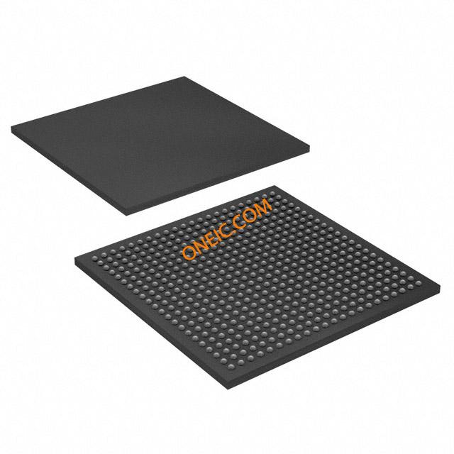
484-FBGA
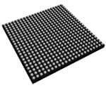
Image Preview

Image Preview