EP2C20F484C6
Cyclone II series FPGAs with 315 I/O, 484-pin FBGA for versatile applications
Manufacturer: altera
series introduction
# Introduction to the EP2C20F484C6 Product Series
## 1. Overview
The EP2C20F484C6 belongs to a highly regarded product series within the field of programmable logic devices (PLDs). Specifically, it is a member of the Cyclone II family of Field - Programmable Gate Arrays (FPGAs) developed by Altera (now Intel). These FPGAs are designed to offer a cost - effective and high - performance solution for a wide range of applications, from consumer electronics to industrial control systems.
## 2. Key Features
### 2.1 Logic Capacity
- The "20" in the EP2C20F484C6 indicates its logic element (LE) count. This FPGA has approximately 20,000 logic elements. Logic elements are the basic building blocks of an FPGA, used to implement combinational and sequential logic functions. With this relatively large number of LEs, it can handle complex digital designs, such as implementing multiple state machines, arithmetic circuits, and data processing algorithms.
### 2.2 Package Type
- The "F484" represents the package type. It comes in a Fine - pitch Ball Grid Array (FBGA) package with 484 pins. The FBGA package offers several advantages. Firstly, it provides a high pin count in a relatively small footprint, which is beneficial for space - constrained applications. Secondly, the ball grid array design allows for better electrical performance, including lower inductance and better heat dissipation compared to some other package types.
### 2.3 Speed Grade
- The "C6" denotes the speed grade of the FPGA. A lower speed grade number generally indicates better performance in terms of propagation delay and maximum operating frequency. The C6 speed grade ensures that the EP2C20F484C6 can operate at relatively high clock frequencies, enabling it to handle high - speed data processing tasks. For example, it can support high - speed serial interfaces and fast - paced digital signal processing algorithms.
### 2.4 Embedded Memory
- This FPGA series includes embedded memory blocks. These memory blocks can be used for various purposes, such as storing data in data - intensive applications, implementing FIFOs (First - In - First - Out buffers), or serving as lookup tables for specific functions. The embedded memory provides a convenient and efficient way to handle data storage and retrieval within the FPGA, reducing the need for external memory in many cases.
### 2.5 Digital Signal Processing (DSP) Blocks
- The EP2C20F484C6 is equipped with dedicated DSP blocks. These blocks are optimized for performing high - speed arithmetic operations, such as multiplication and accumulation, which are commonly used in digital signal processing applications like audio and video processing, wireless communication, and radar systems. The presence of DSP blocks significantly enhances the FPGA's ability to handle complex signal processing tasks.
### 2.6 I/O Capabilities
- It offers a wide range of Input/Output (I/O) pins, which can be configured to support different I/O standards. This flexibility allows the FPGA to interface with various external devices, such as microcontrollers, sensors, and communication modules. The I/O pins can be set to support standards like LVTTL (Low - Voltage Transistor - Transistor Logic), LVCMOS (Low - Voltage Complementary Metal - Oxide - Semiconductor), and differential signaling standards, enabling seamless integration with different types of hardware.
## 3. Applications
### 3.1 Consumer Electronics
- In consumer electronics, the EP2C20F484C6 can be used in devices such as smart TVs, set - top boxes, and gaming consoles. It can handle tasks like video decoding, image processing, and user interface
Images for reference
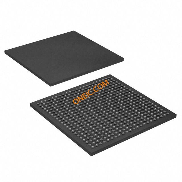
484-FBGA
Image Preview

Image Preview