EP2AGX260FF35C6N
High-density FPGAs for advanced digital circuit design
Manufacturer: altera
series introduction
# Introduction to the EP2AGX260FF35C6N Product Series
## 1. Overview
The EP2AGX260FF35C6N belongs to a high - performance product series that is designed to meet the complex requirements of modern electronic systems. It is a field - programmable gate array (FPGA) device, which offers a unique combination of flexibility, high - speed processing capabilities, and a rich set of features. This makes it an ideal choice for a wide range of applications, from telecommunications and data centers to industrial automation and aerospace.
## 2. Key Features
### 2.1 Logic Capacity
The EP2AGX260FF35C6N boasts a substantial logic capacity. With a large number of configurable logic blocks (CLBs), it can handle highly complex digital designs. These CLBs can be programmed to implement various functions such as arithmetic operations, state machines, and data routing. This high logic capacity allows designers to integrate multiple functions onto a single chip, reducing the overall system cost and board space.
### 2.2 Memory Resources
It is equipped with a significant amount of on - chip memory. This includes block RAM (BRAM) and distributed RAM. The BRAM can be used for storing large amounts of data, such as buffers for data streaming applications. Distributed RAM, on the other hand, is useful for smaller, more local data storage requirements. The availability of these memory resources enables efficient data handling and processing within the FPGA, improving the overall system performance.
### 2.3 High - Speed I/O
The product series features high - speed input/output (I/O) interfaces. These I/O interfaces support a variety of standards, such as LVDS (Low - Voltage Differential Signaling), PCIe (Peripheral Component Interconnect Express), and Ethernet. The high - speed I/O capabilities allow for fast data transfer between the FPGA and external devices, making it suitable for applications that require high - bandwidth communication, such as high - speed data acquisition systems and network switches.
### 2.4 DSP Blocks
The EP2AGX260FF35C6N includes dedicated digital signal processing (DSP) blocks. These blocks are optimized for performing complex mathematical operations, such as multiplication, addition, and filtering. They can be used in applications such as audio and video processing, wireless communication, and radar systems. The presence of DSP blocks significantly enhances the FPGA's ability to handle real - time signal processing tasks.
### 2.5 Power Efficiency
Despite its high performance, the EP2AGX260FF35C6N is designed with power efficiency in mind. It uses advanced power management techniques to reduce power consumption without sacrificing performance. This is particularly important in applications where power consumption is a critical factor, such as battery - powered devices and large - scale data centers.
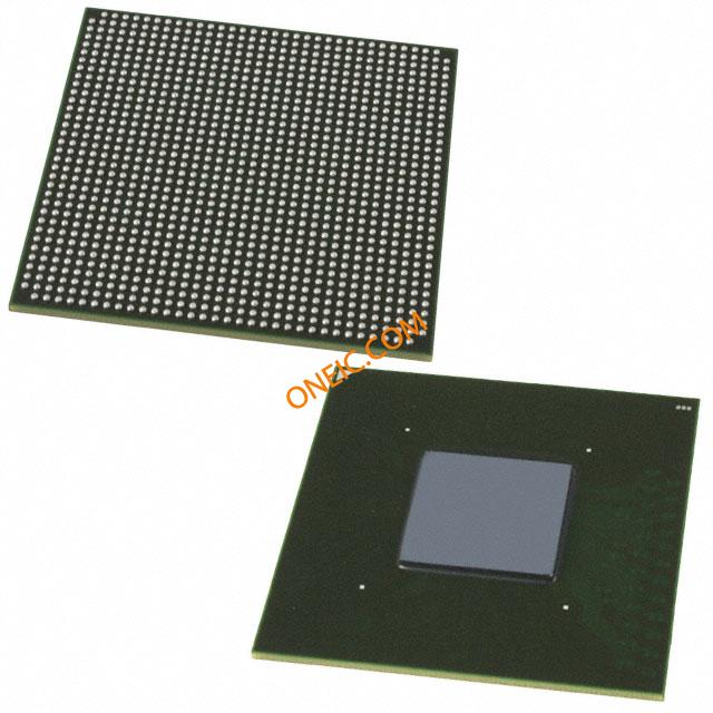
## 3. Package and Pinout
The "FF35" in the product name refers to the package type. The device comes in a fine - pitch ball grid array (FBGA) package, which offers several advantages. The FBGA package provides a large number of pins, allowing for a high - density interconnection between the FPGA and the printed circuit board (PCB). It also has good thermal performance, which helps to dissipate heat generated during operation.
The pinout of the EP2AGX260FF35C6N is carefully designed to ensure easy integration into various systems. The pins are grouped according to their functions, such as power pins, I/O pins, and configuration pins. This makes it easier for designers to connect the FPGA to other components on the PCB and to configure the device during the development process.
## 4. Configuration and Programming
The EP2AGX260FF35C6N can be configured and programmed using industry -
Images for reference
EP2AGX125EF35C4N

Image Preview
Image Preview