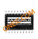
DM74LS373SJ
Octal D-type latch flip-flop for digital circuits
Manufacturer: fairchild
series introduction
# Introduction to the DM74LS373SJ Product Series
## 1. Overview
The DM74LS373SJ belongs to the 74LS series of integrated circuits, which are well - known for their reliability and wide range of applications in digital electronics. This particular product, the DM74LS373SJ, is an octal transparent D - type latch with 3 - state outputs. It is designed to store and transfer digital data in various digital systems, providing a convenient and efficient solution for data handling tasks.
## 2. Key Features
### 2.1 Octal Design
The DM74LS373SJ consists of eight individual D - type latches within a single integrated circuit package. This octal configuration allows it to handle multiple bits of data simultaneously, making it suitable for applications where parallel data processing is required. For example, in a microcontroller - based system, it can be used to latch an 8 - bit data bus, enabling the microcontroller to read or write data in an organized manner.
### 2.2 Transparent Latch Operation
The latches in the DM74LS373SJ are transparent when the latch enable (LE) input is high. In the transparent mode, the output (Q) follows the input (D) directly. When the LE input goes low, the data present at the input at that moment is latched, and the output retains that value until the LE input goes high again or the power is removed. This feature is useful for capturing and holding data at a specific time, such as when a control signal indicates that a particular data value should be stored.
### 2.3 3 - State Outputs
The outputs of the DM74LS373SJ are 3 - state, which means they can be in one of three states: high (logic 1), low (logic 0), or high - impedance (Z). The output enable (OE) input controls the 3 - state operation. When OE is low, the normal output states (high or low) are available. When OE is high, the outputs are in the high - impedance state, effectively disconnecting the device from the external circuit. This feature is crucial in bus - based systems, where multiple devices may share a common data bus. By using the 3 - state outputs, the DM74LS373SJ can be selectively connected or disconnected from the bus, preventing data conflicts.
### 2.4 Low - Power Schottky Technology
The DM74LS373SJ is fabricated using low - power Schottky (LS) technology. This technology offers a good balance between speed and power consumption. Compared to standard TTL (Transistor - Transistor Logic) devices, LS devices consume less power while still providing relatively high - speed operation. This makes the DM74LS373SJ suitable for battery - powered or power - sensitive applications, as well as systems where heat dissipation needs to be minimized.
## 3. Electrical Specifications
### 3.1 Supply Voltage
The DM74LS373SJ typically operates with a supply voltage (VCC) in the range of 4.75V to 5.25V, with a nominal value of 5V. This standard supply voltage makes it compatible with many other digital components in a typical digital system.
### 3.2 Input and Output Voltage Levels
The input voltage levels for a logic 0 are typically in the range of 0V to 0.8V, and for a logic 1, they are in the range of 2V to VCC. The output voltage levels for a logic 0 are typically less than 0.4V, and for a logic 1, they are greater than 2.
Images for reference

Image Preview