CD74HCT08M96
High-speed CMOS quad 2-input AND gate ICs in 14-pin SOIC packaging
Manufacturer: ['harris-semiconductor', 'rochester', 'ti']
series introduction
# CD74HCT08M96 Product Series Introduction
## 1. Overview
The CD74HCT08M96 belongs to the 74HCT family of integrated circuits, which are widely recognized for their high - performance and reliability in digital logic applications. This specific product is a quad 2 - input AND gate, designed to perform basic logical AND operations on digital signals. It combines the advantages of high - speed operation and compatibility with both TTL (Transistor - Transistor Logic) and CMOS (Complementary Metal - Oxide - Semiconductor) logic levels, making it a versatile choice for a variety of electronic systems.
## 2. Key Features
### 2.1 Logic Functionality
- **Quad 2 - Input AND Gates**: The CD74HCT08M96 contains four independent 2 - input AND gates within a single package. Each AND gate has two input pins and one output pin. The output of an AND gate is high (logic 1) only when both of its inputs are high; otherwise, the output is low (logic 0). This basic logical operation is fundamental in digital circuit design, used for tasks such as signal masking, data encoding, and control signal generation.
- **Truth Table**:
| Input A | Input B | Output Y |
| ---- | ---- | ---- |
| 0 | 0 | 0 |
| 0 | 1 | 0 |
| 1 | 0 | 0 |
| 1 | 1 | 1 |
### 2.2 Electrical Characteristics
#### 2.2.1 Power Supply
- **Wide Voltage Range**: It can operate with a power supply voltage (VCC) ranging from 2 V to 6 V. This wide voltage range allows for flexibility in different power supply configurations, making it suitable for a variety of battery - powered and mains - powered applications.
- **Low Power Consumption**: As a CMOS - based device, the CD74HCT08M96 consumes relatively low power compared to some other logic families. This is especially important in portable and battery - operated devices, where power efficiency is crucial for extending battery life.
#### 2.2.2 Speed and Propagation Delay
- **High - Speed Operation**: The device offers fast propagation delays, typically in the range of a few nanoseconds. This high - speed performance enables it to handle high - frequency digital signals, making it suitable for applications that require rapid data processing, such as high - speed communication systems and digital signal processing circuits.
#### 2.2.3 Input and Output Compatibility
- **TTL and CMOS Compatibility**: The CD74HCT08M96 is designed to be compatible with both TTL and CMOS logic levels. Its input thresholds are designed to accept TTL - level signals, while its output levels are compatible with CMOS loads. This compatibility allows it to interface easily with other logic devices from different families, simplifying the design of complex digital systems.
### 2.3 Package and Physical Characteristics
#### 2.3.1 Package Type
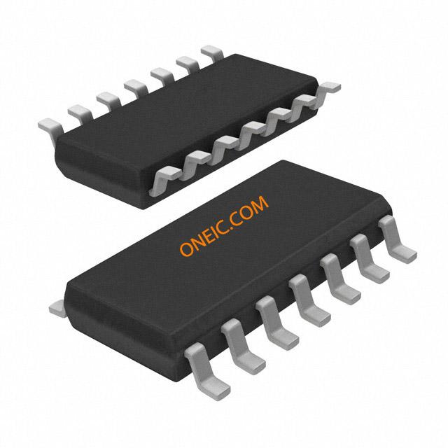
- The CD74HCT08M96 is available in a small - outline integrated circuit (SOIC) package. The SOIC package is a surface - mount package that offers several advantages, including a small footprint, which is beneficial for printed circuit board (PCB) design in compact electronic devices. It also provides good thermal performance and mechanical stability.
#### 2.3.2 Pin Configuration
- The device has a standard pin configuration for a quad 2 - input AND gate. The pins are clearly labeled for easy identification of inputs, outputs, power supply, and ground. This standardization makes it easy to incorporate the CD74HCT08M96 into existing circuit designs
Images for reference

14-SOIC
14-TSSOPa
Image Preview