CD74HC4066PWR
High-speed CMOS quad bilateral analog switches in 14-pin TSSOP
Manufacturer: ti
series introduction
# CD74HC4066PWR Product Series Introduction
## 1. Overview
The CD74HC4066PWR belongs to the 74HC series of integrated circuits, which are high - speed CMOS logic devices. This particular product, the CD74HC4066PWR, is a quad bilateral switch. It combines the advantages of high - speed operation and low power consumption, making it a popular choice in a wide range of electronic applications.
## 2. Package and Pinout
### Package
The "PWR" in the part number indicates that it comes in a TSSOP (Thin Shrink Small Outline Package). This package is relatively small in size, which is beneficial for applications where space is limited, such as in portable electronic devices. The TSSOP package also offers good thermal performance and is suitable for surface - mount technology (SMT) assembly, enabling efficient and automated manufacturing processes.
### Pinout
The CD74HC4066PWR has 16 pins. It contains four independent bilateral switches. Each switch has two signal terminals (input/output) and a control terminal. The pins are carefully arranged to facilitate easy connection in circuit designs. For example, the power supply pins (VCC and GND) are located in positions that allow for straightforward power distribution across the chip, while the input/output and control pins are grouped in a logical manner for each of the four switches.
## 3. Electrical Characteristics
### Power Supply
It operates over a wide range of power supply voltages, typically from 2V to 6V. This wide voltage range provides flexibility in different system designs. For low - power applications, a lower supply voltage can be used to reduce power consumption, while for applications that require higher signal levels or better noise immunity, a higher supply voltage can be selected.
### Input and Output Logic Levels
The input logic levels are compatible with both TTL (Transistor - Transistor Logic) and CMOS logic families. This means that it can be easily interfaced with a variety of other digital circuits. The output logic levels are also well - defined, ensuring reliable signal transmission. The output can source and sink a certain amount of current, which is important for driving other components in the circuit.
### Switching Characteristics
One of the key features of the CD74HC4066PWR is its fast switching speed. The propagation delay time is relatively short, allowing for rapid switching between the on and off states of the switches. This makes it suitable for applications where high - speed signal routing or multiplexing is required. Additionally, the on - resistance of the switches is low, which minimizes signal attenuation and distortion when the switch is in the on state.
## 4. Functional Description
### Quad Bilateral Switch Operation
As a quad bilateral switch, the CD74HC4066PWR contains four independent switches. Each switch can be controlled independently by applying a logic high or low signal to its corresponding control terminal. When the control signal is high, the switch is closed, allowing the signal to pass between the two input/output terminals. When the control signal is low, the switch is open, isolating the two terminals from each other.
### Signal Routing and Multiplexing
These switches can be used for signal routing in various circuits. For example, in a data acquisition system, they can be used to select different input channels. They can also be used in audio and video signal processing circuits to switch between different sources or destinations. In multiplexing applications, the CD74HC4066PWR can be used to combine multiple input signals into a single output or vice versa.
## 5. Applications
### Consumer Electronics
In portable audio players, the CD74HC4066PWR can be used to switch between different audio sources, such
Images for reference
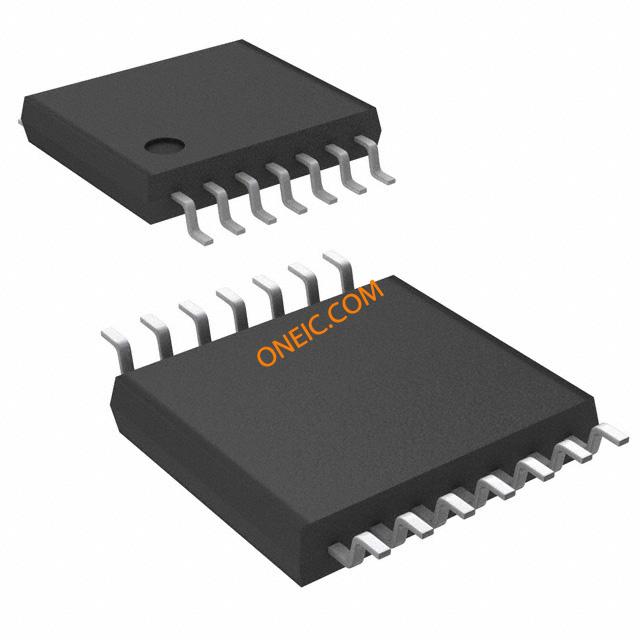
14-TSSOP
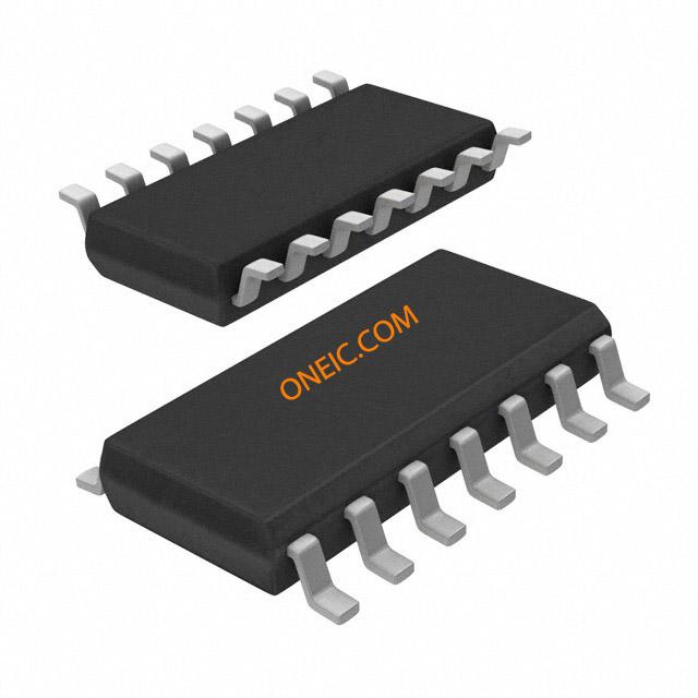
14-TSSOPa
Image Preview