CD74HC4051PWR
High-speed CMOS analog multiplexer/demultiplexer ICs in TSSOP packages
Manufacturer: ti
series introduction
# CD74HC4051PWR Product Series Introduction
## 1. Overview
The CD74HC4051PWR belongs to the 74HC series of integrated circuits, which are high - speed CMOS logic devices. This particular product, the CD74HC4051PWR, is an 8 - channel analog multiplexer/demultiplexer. It combines the advantages of high - speed operation and low power consumption, making it a popular choice in a wide range of electronic applications.
## 2. Key Features
### 2.1 Electrical Characteristics
- **Supply Voltage Range**: It can operate within a relatively wide supply voltage range, typically from 2V to 6V. This flexibility allows it to be used in various power - supply environments, whether it's a battery - powered device with a lower voltage or a standard 5V power - supply system.
- **Low Power Consumption**: As a CMOS device, the CD74HC4051PWR consumes very little power. This is crucial for battery - operated devices, as it helps to extend the battery life. The low power consumption also results in less heat generation, which can improve the overall reliability of the system.
- **High - Speed Operation**: It offers high - speed switching capabilities, with typical propagation delays in the range of a few nanoseconds. This makes it suitable for applications where fast signal routing is required, such as in high - speed data acquisition systems.
### 2.2 Input/Output Characteristics
- **Analog and Digital Compatibility**: The CD74HC4051PWR can handle both analog and digital signals. It can be used to route analog signals, such as audio or video signals, as well as digital signals, like control signals or data signals.
- **High Input Impedance**: The inputs of the device have a high impedance, which means that they draw very little current from the source. This is beneficial as it minimizes the loading effect on the input signals, ensuring that the signal integrity is maintained.
- **Output Drive Capability**: It has sufficient output drive capability to drive standard loads. The output can source and sink a certain amount of current, allowing it to interface with other components in the circuit, such as microcontrollers, amplifiers, or other logic gates.
### 2.3 Package and Pinout
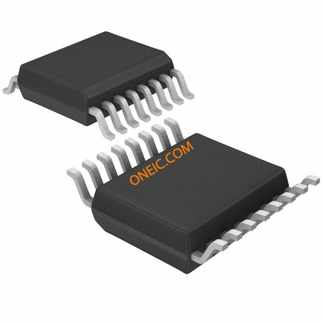
- **Package Type**: The CD74HC4051PWR comes in a PowerPAD TSSOP (Thin Shrink Small Outline Package) package. This package is compact, which is suitable for applications where space is limited, such as in portable devices. The PowerPAD feature helps to improve the thermal performance of the device by providing a better heat - dissipation path.
- **Pinout Configuration**: The device has a well - defined pinout. It has three address inputs (A0, A1, A2) that are used to select one of the eight input/output channels. There is also an enable input (INH) that can be used to disable the device. The common terminal (Z) is used for both multiplexing and demultiplexing operations.
## 3. Functional Description
### 3.1 Multiplexer Operation
In multiplexer mode, the CD74HC4051PWR selects one of the eight input channels (Y0 - Y7) based on the binary code applied to the address inputs (A0, A1, A2). For example, if the address inputs are set to 000, the signal on input channel Y0 will be routed to the common output terminal Z. The enable input (INH) can be used to disable the multiplexer. When INH is high, the output Z is in a high - impedance state, effectively disconnecting it from all the input
Images for reference
16-TSSOP

Image Preview
Image Preview