BU4094BCF
8-bit shift and store registers in compact 16-pin packages
Manufacturer: rohm
series introduction
# Introduction to the BU4094BCF Product Series
## 1. Overview
The BU4094BCF product series is a remarkable line of integrated circuits that offers a wide range of applications in the field of electronics. These devices are designed with high - performance and reliability in mind, catering to the needs of both hobbyists and professional engineers working on various projects.
## 2. Key Features
### 2.1 Logic Functionality
The BU4094BCF is a 8 - stage shift register with a strobe input and an output enable function. It can be used to convert parallel data to serial data and vice versa. This makes it extremely useful in applications where data needs to be transferred between different parts of a circuit in an organized and efficient manner. For example, in a display system, it can be used to shift out data to multiple LEDs or other display elements one by one.
### 2.2 Compatibility
These integrated circuits are designed to be compatible with a wide range of logic families. They can operate with TTL (Transistor - Transistor Logic) and CMOS (Complementary Metal - Oxide - Semiconductor) logic levels. This compatibility allows for seamless integration into existing circuits that may use different logic technologies, providing flexibility in circuit design.
### 2.3 High - Speed Operation
The BU4094BCF series is capable of high - speed data transfer. It has a fast clock frequency response, which enables it to handle large amounts of data in a short period. This is crucial in applications such as high - speed communication systems, where data needs to be transmitted and processed rapidly.
### 2.4 Low Power Consumption
In today's energy - conscious world, the low power consumption of the BU4094BCF is a significant advantage. The CMOS technology used in these devices ensures that they draw minimal power during operation. This not only reduces the overall power requirements of the system but also helps in extending the battery life in portable applications.
### 2.5 Output Drive Capability
The outputs of the BU4094BCF have a reasonable drive capability. They can directly drive small - to - medium - sized loads such as LEDs, relays, and small motors. This eliminates the need for additional buffer circuits in many cases, simplifying the circuit design and reducing the component count.
## 3. Pin Configuration
The BU4094BCF typically comes in a standard DIP (Dual In - Line Package) or SOIC (Small Outline Integrated Circuit) package. The pinout is well - defined and easy to understand.
- **Data Input (D)**: This pin is used to input the data that will be shifted into the register.
- **Clock Input (CP)**: The clock signal applied to this pin controls the shifting of data through the register. Each rising or falling edge of the clock (depending on the device's design) causes the data to move one stage further in the register.
- **Strobe Input (ST)**: The strobe input is used to control when the parallel outputs are updated. When the strobe is active, the data in the register is transferred to the parallel outputs.
- **Output Enable (OE)**: This pin is used to enable or disable the outputs. When the output enable is active, the data at the parallel outputs is available; otherwise, the outputs are in a high - impedance state.
- **Parallel Outputs (Q0 - Q7)**: These pins provide the parallel representation of the data stored in the register.
- **Serial Output (Q7S)**: This pin provides the serial output of the last stage of the register, which can be used for further data transmission.
## 4. Applications
### 4.1 Display Systems
As mentioned earlier, the BU409
Images for reference
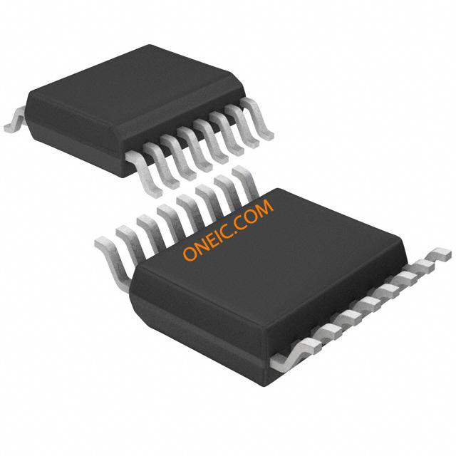
16-SSOP
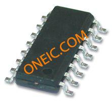
Image Preview
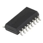
Image Preview