ADS8556IPMR
16-bit, 630kSPS, 6-channel simultaneous sampling analog-to-digital converter
Manufacturer: ti
series introduction
# ADS8556IPMR Product Series Introduction
## 1. Overview
The ADS8556IPMR is a high - performance analog - to - digital converter (ADC) product series offered by Texas Instruments. This series is designed to meet the demanding requirements of various applications that need accurate and fast conversion of analog signals to digital data. With its advanced features and reliable performance, it has become a popular choice in many industries.
## 2. Key Features
### High - Resolution Conversion
The ADS8556IPMR provides a high - resolution conversion of up to 16 bits. This high resolution allows for the precise measurement of analog signals, enabling applications to detect even the smallest changes in the input signal. For example, in sensor applications where the measured physical quantity may have very small variations, the 16 - bit resolution ensures that these changes are accurately captured and converted into digital values.
### Fast Sampling Rate
It offers a relatively fast sampling rate, which is crucial for applications that require real - time data acquisition. The ability to sample analog signals at a high rate allows the ADC to capture rapid changes in the input signal. In applications such as audio processing or high - speed data acquisition systems, the fast sampling rate ensures that the digital representation of the analog signal is as accurate as possible, minimizing signal distortion.
### Low Power Consumption
Power efficiency is an important consideration in many modern electronic systems. The ADS8556IPMR is designed with low power consumption in mind. This makes it suitable for battery - powered devices or applications where power management is critical. By consuming less power, the product helps to extend the battery life of portable devices and reduces the overall energy consumption of the system.
### Wide Input Voltage Range
The product series supports a wide input voltage range. This flexibility allows it to be used with a variety of analog signals, whether they are low - voltage signals from sensors or higher - voltage signals from other analog sources. The wide input voltage range eliminates the need for additional signal conditioning circuits in many cases, simplifying the overall system design.
### On - Chip Reference
The ADS8556IPMR comes with an on - chip reference voltage source. This on - chip reference provides a stable and accurate voltage reference for the ADC conversion process. It eliminates the need for an external reference voltage source, reducing the component count and cost of the system. Additionally, the on - chip reference ensures better performance and reliability as it is integrated with the ADC, minimizing the effects of external noise and interference.
## 3. Functional Block Diagram and Working Principle
### Block Diagram
The main components of the ADS8556IPMR include an analog input stage, a sample - and - hold circuit, an ADC core, and a digital output interface. The analog input stage is responsible for receiving the analog signals from the external source. The sample - and - hold circuit samples the analog signal at a specific time and holds its value during the conversion process. The ADC core then converts the held analog value into a digital code using a specific conversion algorithm. Finally, the digital output interface transfers the converted digital data to the external microcontroller or other digital devices.
### Working Principle
When an analog signal is applied to the input of the ADS8556IPMR, the sample - and - hold circuit samples the signal at the sampling instant determined by the internal clock. Once the signal is held, the ADC core starts the conversion process. The 16 - bit conversion is typically based on a successive - approximation register (SAR) algorithm. The SAR ADC compares the input voltage with a series of reference voltages generated internally and determines the digital code that represents the input voltage. After the conversion is complete, the digital code is available at the output pins of the ADC and can be read by the external device.
## 4. Applications
### Industrial Automation
In industrial automation systems,
Images for reference
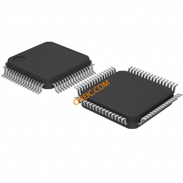
64-LQFP
Image Preview
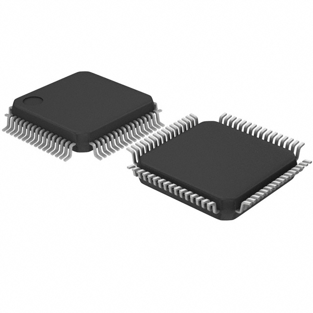
Image Preview