ADC124S101CIMM
12-bit analog-to-digital converters with 4 channels, 1Msps, in MSOP-10 package
Manufacturer: ['national-semiconductor', 'rochester', 'ti']
series introduction
# Introduction to the ADC124S101CIMM Product Series
## 1. Overview
The ADC124S101CIMM is a highly advanced and versatile analog - to - digital converter (ADC) product series designed to meet the demanding requirements of modern electronic systems. ADCs play a crucial role in converting real - world analog signals, such as voltage, current, or temperature, into digital data that can be processed by microcontrollers, digital signal processors (DSPs), and other digital devices. This product series offers a combination of high performance, precision, and flexibility, making it suitable for a wide range of applications across various industries.
## 2. Key Features
### 2.1 High - Resolution Conversion
The ADC124S101CIMM features a 12 - bit resolution, which means it can distinguish between 4096 different levels of the input analog signal. This high resolution allows for accurate and detailed representation of the analog input, enabling precise measurement and control in applications where fine - grained data is essential.
### 2.2 Fast Sampling Rate
With a sampling rate of up to [X] kilosamples per second (ksps), the ADC124S101CIMM can quickly capture and convert analog signals. This fast sampling rate is particularly useful in applications that require real - time data acquisition, such as audio processing, sensor monitoring, and communication systems.
### 2.3 Low Power Consumption
In today's energy - conscious world, power efficiency is a critical factor. The ADC124S101CIMM is designed with low power consumption in mind. It operates at a relatively low supply voltage and has power - saving modes that can be enabled to reduce power consumption during idle periods. This makes it an ideal choice for battery - powered devices and other applications where power conservation is a priority.
### 2.4 Wide Input Voltage Range
The product series supports a wide input voltage range, typically from [Vmin] to [Vmax]. This wide range allows it to handle a variety of analog signals without the need for extensive signal conditioning. It can directly interface with different types of sensors and other analog sources, simplifying the design process and reducing the overall system cost.
### 2.5 Serial Interface
The ADC124S101CIMM is equipped with a serial interface, such as SPI (Serial Peripheral Interface). The serial interface provides a simple and efficient way to communicate with the ADC, allowing for easy integration into existing digital systems. It also enables multiple ADCs to be daisy - chained together, further expanding the system's capabilities.
## 3. Functional Block Diagram and Operation
The ADC124S101CIMM consists of several key functional blocks, including an input buffer, a sample - and - hold circuit, an analog - to - digital conversion core, and a serial interface.
### 3.1 Input Buffer
The input buffer is responsible for isolating the ADC from the input source and providing a high - impedance input. This helps to prevent loading effects on the input signal and ensures accurate signal acquisition.
### 3.2 Sample - and - Hold Circuit
The sample - and - hold circuit samples the input analog signal at a specific time instant and holds its value constant during the conversion process. This is necessary because the analog - to - digital conversion takes a finite amount of time, and the input signal may change during this period.
### 3.3 Analog - to - Digital Conversion Core
The analog - to - digital conversion core is the heart of the ADC. It uses a successive - approximation register (SAR) algorithm to convert the held analog voltage into a 12 - bit digital code. The SAR algorithm compares the input voltage with a series of reference voltages and
Images for reference
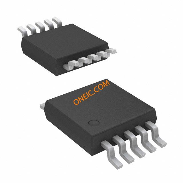
10-MSOP
Image Preview
Image Preview