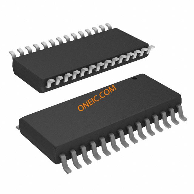
AD9850BRSZ
125MHz direct digital synthesizer ICs in 28-pin SSOP format
Manufacturer: ['rochester', 'analog-devices']
series introduction
# AD9850BRSZ Product Series Introduction
## 1. Overview
The AD9850BRSZ is a highly versatile and widely - used direct digital synthesizer (DDS) product series developed by Analog Devices. DDS technology is a key method for generating high - precision, programmable analog signals, and the AD9850BRSZ stands out in the market due to its excellent performance, flexibility, and cost - effectiveness.
## 2. Key Features
### 2.1 High - Frequency Output
The AD9850BRSZ can generate output frequencies up to 125 MHz. This high - frequency capability makes it suitable for a wide range of applications, including radio frequency (RF) signal generation, wireless communication systems, and test and measurement equipment.
### 2.2 High - Resolution Frequency Tuning
It offers a frequency tuning resolution of up to 0.0291 Hz at a 125 MHz system clock. This extremely high resolution allows for very precise frequency adjustments, which is crucial in applications such as frequency - hopping spread - spectrum (FHSS) communication, where accurate frequency control is necessary for reliable data transmission.
### 2.3 Programmable Phase Control
In addition to frequency tuning, the AD9850BRSZ provides programmable phase control. The phase can be adjusted in steps of 11.25 degrees, enabling users to fine - tune the phase relationship between different signals. This feature is useful in applications such as beamforming in antenna arrays, where phase control is used to steer the radiation pattern.
### 2.4 Low - Power Consumption
The device is designed with low - power operation in mind. It can operate on a single +5V power supply, making it suitable for battery - powered applications. The low - power consumption also helps to reduce heat dissipation, which is beneficial for the long - term reliability of the device.
### 2.5 Serial and Parallel Interface
The AD9850BRSZ supports both serial and parallel data input interfaces. The parallel interface allows for fast data transfer, which is useful when rapid frequency or phase changes are required. The serial interface, on the other hand, is more suitable for applications where the number of available pins is limited, such as in small - form - factor devices.
## 3. Functional Block Diagram and Working Principle
### 3.1 Functional Block Diagram
The AD9850BRSZ consists of several key functional blocks, including a phase accumulator, a sine lookup table, a digital - to - analog converter (DAC), and a low - pass filter.
- **Phase Accumulator**: It accumulates the frequency tuning word (FTW) at each clock cycle. The output of the phase accumulator represents the phase of the generated signal.
- **Sine Lookup Table**: The phase value from the phase accumulator is used as an address to look up the corresponding sine amplitude value in the sine lookup table.
- **Digital - to - Analog Converter (DAC)**: The digital sine amplitude value from the lookup table is converted into an analog signal by the DAC.
- **Low - Pass Filter**: The output of the DAC contains high - frequency components due to the sampling process. The low - pass filter is used to remove these high - frequency components and produce a smooth analog sine wave.
### 3.2 Working Principle
The user can program the frequency tuning word and phase control word into the AD9850BRSZ through the serial or parallel interface. The phase accumulator then accumulates the frequency tuning word at each clock cycle, which determines the rate at which the phase of the output signal changes. The sine lookup table maps the phase value to a corresponding sine amplitude value, and the DAC converts this digital value into an analog signal.
Images for reference
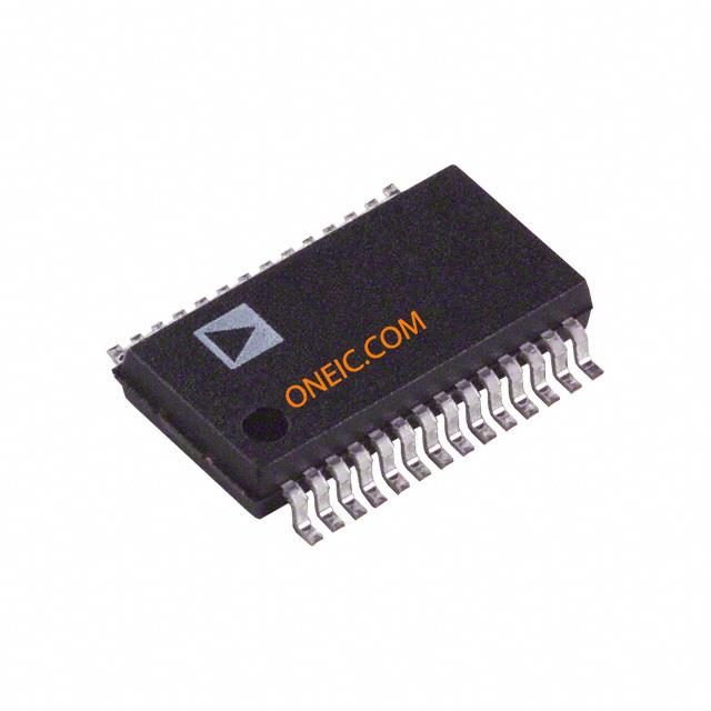
505-28-SSOP
28-SOIC
Image Preview