AD9516-3BCPZ
64-pin clock generators with integrated PLL and VCO for precision timing
Manufacturer: ['rochester', 'analog-devices']
series introduction
# AD9516 - 3BCPZ Product Series Introduction
## 1. Overview
The AD9516 - 3BCPZ is a highly advanced and versatile clock generator and jitter cleaner product series developed by Analog Devices. This series is designed to meet the demanding requirements of modern high - performance electronic systems, offering precise clock generation and distribution capabilities with excellent jitter performance. It plays a crucial role in a wide range of applications, including telecommunications, data centers, test and measurement equipment, and high - speed digital systems.
## 2. Key Features
### 2.1 High - Performance Clock Generation
- **Multiple Outputs**: The AD9516 - 3BCPZ provides a rich set of clock outputs. It can generate up to 12 differential or 24 single - ended clock outputs, allowing it to drive multiple components within a system simultaneously. This feature is particularly useful in complex systems where different parts require different clock frequencies.
- **Wide Frequency Range**: It supports a wide frequency range for both input and output clocks. The input reference frequency can range from a few kilohertz to several hundred megahertz, and the output frequencies can be programmed to cover a broad spectrum, enabling it to adapt to various system requirements.
### 2.2 Low Jitter Performance
- **Excellent Phase Noise Characteristics**: Jitter is a critical parameter in high - speed digital systems as it can cause errors in data transmission and reception. The AD9516 - 3BCPZ is engineered to have extremely low jitter, with typical phase noise performance in the range of - 150 dBc/Hz at 10 kHz offset for a 100 MHz output clock. This low jitter ensures reliable and accurate operation of high - speed interfaces such as PCIe, Ethernet, and Serial ATA.
### 2.3 Programmability
- **Flexible Configuration**: The device can be easily programmed through its serial peripheral interface (SPI). Users can configure various parameters such as output frequencies, output phases, and output drive strengths. This flexibility allows system designers to optimize the clock generation according to the specific requirements of their applications.
- **On - Chip Memory**: It has on - chip non - volatile memory, which can store the configuration settings. This means that once the device is programmed, it can retain the settings even after power cycling, eliminating the need for repeated programming during system startup.
### 2.4 Power Management
- **Low Power Consumption**: In today's energy - conscious world, power consumption is an important consideration. The AD9516 - 3BCPZ is designed to operate with relatively low power consumption, making it suitable for battery - powered devices and energy - efficient systems. It also offers power - down modes that can further reduce power consumption when the device is not in use.
## 3. Functional Block Diagram and Operation
### 3.1 Input Stage
The input stage of the AD9516 - 3BCPZ accepts one or more reference clock signals. These reference clocks can be derived from crystal oscillators, external clock sources, or other stable frequency references. The device has built - in input buffers that can handle different types of input signals, including differential and single - ended signals.
### 3.2 Phase - Locked Loop (PLL)
At the heart of the AD9516 - 3BCPZ is a high - performance phase - locked loop. The PLL takes the input reference clock and multiplies or divides it to generate the desired output frequencies. It uses a voltage - controlled oscillator (VCO) to generate a high - frequency signal, which is then divided and filtered to produce the output clocks. The PLL has a fast lock - in time, ensuring that the output clocks are stable and accurate within a short period.
Images for reference
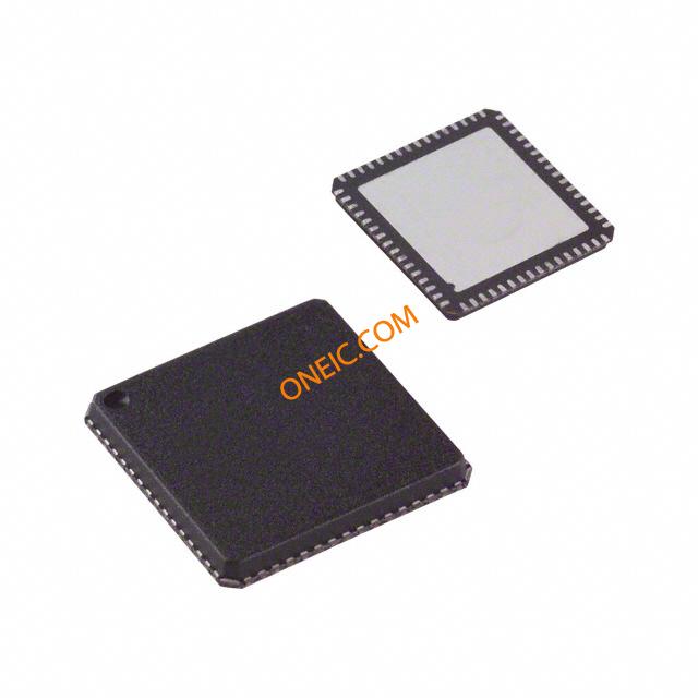
64-LF Pkg
Image Preview
Image Preview