AD9513BCPZ
Compact 32-pin clock distribution ICs with 800 MHz frequency support
Manufacturer: ['rochester', 'analog-devices']
series introduction
# AD9513BCPZ Product Series Introduction
## 1. Overview
The AD9513BCPZ is a high - performance clock generator and synthesizer product series developed by Analog Devices. It is designed to meet the demanding requirements of modern electronic systems, providing accurate and stable clock signals for a wide range of applications. With its advanced features and excellent performance, the AD9513BCPZ has become a popular choice in various industries such as telecommunications, data centers, test and measurement, and industrial automation.
## 2. Key Features
### 2.1 High - Frequency Generation
- The AD9513BCPZ is capable of generating high - frequency clock signals up to a certain range (specific frequency limits can be found in the detailed datasheet). This high - frequency capability makes it suitable for applications that require fast data transfer rates and high - speed processing, such as high - speed serial interfaces in telecommunications equipment.
- It can generate multiple output frequencies simultaneously, allowing it to support different components within a system that may require different clock frequencies.
### 2.2 Low Jitter Performance
- Jitter is a critical parameter in clock generation, as it can affect the accuracy and reliability of data transmission and processing. The AD9513BCPZ features extremely low jitter characteristics, which ensures clean and stable clock signals.
- Low jitter is especially important in applications such as high - definition video transmission, where even small amounts of jitter can cause visible artifacts in the video output.
### 2.3 Programmability
- One of the significant advantages of the AD9513BCPZ is its high degree of programmability. Users can configure various parameters such as output frequencies, phase relationships, and output levels through a simple programming interface.
- This programmability allows for flexibility in system design, enabling engineers to adapt the clock generator to different system requirements without the need for significant hardware changes.
### 2.4 Multiple Outputs
- The product series offers multiple clock outputs, which can be used to drive different parts of a system. These outputs can be configured independently, providing the flexibility to meet the diverse clocking needs of complex electronic systems.
- For example, in a data center server, different components such as the CPU, memory, and network interface cards may require different clock signals, and the multiple outputs of the AD9513BCPZ can easily satisfy these requirements.
### 2.5 Power Management
- The AD9513BCPZ is designed with power management in mind. It offers low - power operation modes, which can help reduce the overall power consumption of the system.
- This is particularly important in battery - powered devices or large - scale systems where power efficiency is a key consideration.
## 3. Functional Block Diagram and Working Principle
### 3.1 Input Stage
- The AD9513BCPZ accepts one or more reference clock inputs. These reference clocks serve as the basis for generating all the output clock signals. The reference clocks can be from external crystal oscillators, voltage - controlled oscillators (VCOs), or other clock sources.
### 3.2 Phase - Locked Loop (PLL)
- Inside the device, a phase - locked loop is used to multiply and divide the reference clock frequencies to generate the desired output frequencies. The PLL compares the phase of the reference clock with the phase of a feedback signal from the output, and then adjusts the VCO frequency to minimize the phase difference.
- This ensures that the output clock signals are accurately synchronized with the reference clock and have the desired frequency and phase relationships.
### 3.3 Output Buffers
- The generated clock signals are then passed through output buffers. These buffers provide sufficient drive strength to drive external loads, such as integrated circuits, printed circuit board traces,
Images for reference

32-VFQFN
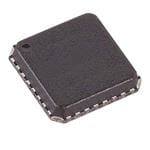
Image Preview
Image Preview