AD9467BCPZ-250
16-bit high-speed analog-to-digital converters with LVDS interface
Manufacturer: analog-devices
series introduction
# AD9467BCPZ - 250: A High - Performance Analog - to - Digital Converter Product Series
## 1. Overview
The AD9467BCPZ - 250 is a remarkable member of Analog Devices' high - speed analog - to - digital converter (ADC) product series. This ADC is engineered to meet the demanding requirements of a wide range of applications, from high - end communication systems to advanced instrumentation and test equipment. Its high - speed conversion capabilities, excellent signal - to - noise ratio (SNR), and low power consumption make it a top choice for designers seeking high - performance data acquisition solutions.
## 2. Key Features
### 2.1 High - Speed Sampling
The "250" in the part number indicates its sampling rate. The AD9467BCPZ - 250 can sample analog signals at a rate of up to 250 megasamples per second (MSPS). This high sampling rate enables it to accurately capture high - frequency analog signals, making it suitable for applications such as wideband communication systems, where rapid data conversion is essential to handle large amounts of information.
### 2.2 High Resolution
It offers a 16 - bit resolution, which means it can distinguish between 2^16 (65,536) different voltage levels. This high resolution allows for precise digitization of analog signals, resulting in more accurate representation of the original signal. In applications like medical imaging and high - precision instrumentation, the ability to capture fine details in the analog signal is crucial, and the 16 - bit resolution of the AD9467BCPZ - 250 meets this requirement effectively.
### 2.3 Excellent Signal - to - Noise Ratio (SNR)
The ADC provides a high SNR of up to 75 dBFS (decibels full - scale). A high SNR indicates that the converter can accurately convert the analog signal into a digital representation while minimizing the amount of noise introduced during the conversion process. This is particularly important in applications where the signal of interest may be weak, such as in radio astronomy or low - level sensor measurements.
### 2.4 Low Power Consumption
Despite its high - speed and high - performance capabilities, the AD9467BCPZ - 250 is designed with power efficiency in mind. It consumes relatively low power, which is beneficial for battery - powered devices or systems where power consumption is a critical factor. This low power consumption also helps in reducing heat generation, which can improve the overall reliability and longevity of the system.
### 2.5 Flexible Input Range
The ADC has a flexible input range, allowing it to handle a variety of analog signal amplitudes. This flexibility makes it adaptable to different types of input signals, whether they are from low - level sensors or high - power communication signals. Designers can easily configure the input range to match the characteristics of the specific application, enhancing the versatility of the product.
## 3. Functional Block Diagram and Working Principle
### 3.1 Input Stage
The input stage of the AD9467BCPZ - 250 is designed to accept analog signals. It includes an input buffer that provides impedance matching and isolation between the input signal source and the internal conversion circuitry. This helps in minimizing signal distortion and ensuring accurate signal acquisition.
### 3.2 Sampling and Hold Circuit
The sampling and hold circuit samples the analog input signal at the specified sampling rate (250 MSPS in this case) and holds the sampled value constant during the conversion process. This is necessary because the subsequent analog - to - digital conversion takes a finite amount of time, and the sampled value needs to remain stable for accurate conversion.
### 3.3 Analog - to - Digital Conversion
Images for reference
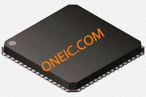
Image Preview
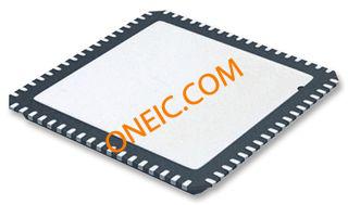
Image Preview
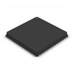
Image Preview