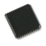
AD9265BCPZ-80
High-speed 16-bit analog-to-digital converters for precision signal processing
Manufacturer: analog-devices
series introduction
# AD9265BCPZ - 80 Product Series Introduction
## 1. Overview
The AD9265BCPZ - 80 is a high - performance analog - to - digital converter (ADC) product series developed by Analog Devices. This series is designed to meet the demanding requirements of a wide range of applications, including communication systems, instrumentation, and test equipment. With its advanced technology and excellent performance characteristics, the AD9265BCPZ - 80 offers a reliable solution for converting analog signals into digital data accurately and efficiently.
## 2. Key Features
### 2.1 High - Speed Conversion
The "80" in the model name indicates that the AD9265BCPZ - 80 has a sampling rate of up to 80 MSPS (Mega Samples Per Second). This high - speed sampling capability allows it to capture rapidly changing analog signals, making it suitable for applications such as high - speed data acquisition and wide - band communication systems.
### 2.2 High Resolution
It provides a 14 - bit resolution, which means it can distinguish between 2^14 (16,384) different levels of the input analog signal. This high resolution enables the accurate representation of the input signal, reducing quantization errors and providing more detailed information about the signal's characteristics.
### 2.3 Low Power Consumption
In today's energy - conscious world, power consumption is a crucial factor. The AD9265BCPZ - 80 is designed with low - power technology, which helps to reduce the overall power consumption of the system. This is especially important for battery - powered devices or applications where heat dissipation is a concern.
### 2.4 Excellent Signal - to - Noise Ratio (SNR)
The ADC offers a high SNR, typically around 72 dBFS (decibels full - scale). A high SNR indicates that the ADC can accurately capture the input signal while minimizing the impact of noise. This is essential for applications where the quality of the digital output is critical, such as in medical imaging and high - precision measurement systems.
### 2.5 Wide Input Voltage Range
It has a wide input voltage range, which allows it to handle a variety of analog signals. This flexibility makes it suitable for different types of input sources, whether they are low - level signals from sensors or high - level signals from communication transmitters.
## 3. Functional Block Diagram and Working Principle
### 3.1 Block Diagram
The AD9265BCPZ - 80 consists of several key functional blocks, including an input buffer, a sample - and - hold circuit, an analog - to - digital conversion core, and an output driver. The input buffer is used to isolate the input signal from the internal circuitry of the ADC, ensuring that the input impedance remains constant and minimizing the loading effect on the input source. The sample - and - hold circuit samples the input analog signal at the specified sampling rate and holds it constant during the conversion process. The analog - to - digital conversion core then converts the held analog signal into a digital code using a successive - approximation register (SAR) algorithm. Finally, the output driver buffers the digital output and provides it to the external system.
### 3.2 Working Principle
When an analog signal is applied to the input of the AD9265BCPZ - 80, the input buffer amplifies and conditions the signal. The sample - and - hold circuit then takes a snapshot of the input signal at each sampling instant. The SAR algorithm in the conversion core compares the held analog voltage with a series of reference voltages and determines the digital code that best represents the input voltage. This digital code is then outputted through the output driver, which can be connected to a microcontroller, a
Images for reference
.jpg)
48-QFN

Image Preview