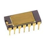
AD536ASD
True RMS to DC converter ICs for voltage regulation and data acquisition
Manufacturer: analog-devices
series introduction
# AD536ASD Product Series Introduction
## 1. Overview
The AD536ASD is a highly versatile and reliable integrated circuit product series offered by Analog Devices. This series is specifically designed to meet a wide range of signal - processing requirements in various electronic applications. With its advanced technology and excellent performance characteristics, the AD536ASD has become a popular choice among engineers and designers.
## 2. Key Features
### 2.1 True RMS - to - DC Conversion
One of the most significant features of the AD536ASD is its ability to perform true root - mean - square (RMS) to direct - current (DC) conversion. In many real - world applications, electrical signals are complex and non - sinusoidal. Traditional average - responding converters may not accurately measure the power or amplitude of such signals. The AD536ASD, however, can accurately calculate the RMS value of any input waveform, including sine waves, square waves, triangular waves, and even random noise. This makes it ideal for applications where accurate power measurement, signal amplitude monitoring, and distortion analysis are required.
### 2.2 Wide Input Frequency Range
The AD536ASD supports a wide input frequency range, typically from DC up to several hundred kilohertz. This broad frequency response allows it to handle a diverse set of input signals, whether they are low - frequency audio signals or high - frequency communication signals. It provides flexibility for use in different types of systems, such as audio amplifiers, radio frequency (RF) receivers, and power monitoring equipment.
### 2.3 High Accuracy and Low Drift
Accuracy is crucial in signal - processing applications. The AD536ASD offers high - precision RMS - to - DC conversion with low error rates. It also has low temperature drift characteristics, which means that its performance remains stable over a wide temperature range. This stability ensures consistent and reliable operation in different environmental conditions, reducing the need for frequent calibration and improving the overall system performance.
### 2.4 Low Power Consumption
In today's energy - conscious world, power consumption is an important consideration. The AD536ASD is designed to operate with relatively low power consumption. This makes it suitable for battery - powered devices and other applications where power efficiency is a priority. By minimizing power usage, it helps to extend the battery life of portable devices and reduces the overall energy cost of the system.
### 2.5 Small Package Size
The AD536ASD is available in a compact package, which saves board space in electronic designs. Its small form factor makes it easy to integrate into densely populated printed circuit boards (PCBs), enabling the development of more compact and lightweight electronic products. This is particularly beneficial for applications such as handheld devices, where space is at a premium.
## 3. Functional Block Diagram and Working Principle
### 3.1 Block Diagram
The AD536ASD consists of several key functional blocks, including an input amplifier, a squaring circuit, an averaging circuit, and a square - root circuit. The input amplifier is responsible for amplifying the input signal to an appropriate level for further processing. The squaring circuit squares the amplified input signal, and the averaging circuit calculates the average value of the squared signal over a certain period. Finally, the square - root circuit takes the square root of the averaged squared signal to obtain the RMS value, which is then output as a DC voltage.
### 3.2 Working Principle
When an input signal is applied to the AD536ASD, it first passes through the input amplifier. The amplified signal is then squared, which effectively eliminates the negative part of the waveform and emphasizes the magnitude of the signal. The averaging circuit integrates the squared signal over time to obtain the mean - squared value. Taking the square root of this mean
Images for reference

505-14-CDIP

Image Preview