74LVC2244APW,118
Quad and octal buffer/driver ICs in 20-pin TSSOP packages
Manufacturer: ['nexperia', 'nxp']
series introduction
# Introduction to the 74LVC2244APW,118 Product Series
## 1. Overview
The 74LVC2244APW,118 belongs to the 74LVC logic family, which is well - known for its high - performance, low - voltage operation, and compatibility with a wide range of digital systems. This specific product is an octal buffer/line driver with 3 - state outputs, designed to provide efficient signal buffering and driving capabilities in various electronic applications.
## 2. Key Features
### 2.1 Low - Voltage Operation
- It operates at a supply voltage range of 1.65V to 3.6V. This low - voltage requirement makes it suitable for battery - powered devices, where power consumption needs to be minimized. For example, in portable consumer electronics such as smartwatches or wireless earbuds, the low - voltage operation helps to extend the battery life.
### 2.2 High - Speed Performance
- The device offers high - speed switching characteristics, with typical propagation delays in the range of a few nanoseconds. This allows it to handle high - frequency signals effectively, making it ideal for applications in high - speed data communication systems, like USB interfaces or high - speed serial buses.
### 2.3 3 - State Outputs
- The 3 - state outputs provide an additional level of flexibility. In the high - impedance state, the outputs are effectively disconnected from the circuit, allowing multiple devices to share the same bus without interference. This feature is crucial in bus - based systems, such as in computer motherboards where multiple components need to communicate over a common data bus.
### 2.4 Wide Input Voltage Tolerance
- It can tolerate input voltages from 0V to VCC, which means it can interface with different logic levels. This makes it easy to integrate with other components that may have different voltage requirements, enhancing its compatibility in mixed - voltage systems.
## 3. Pin Configuration and Functionality
### 3.1 Pinout
The 74LVC2244APW,118 comes in a specific package, typically a TSSOP (Thin Shrink Small Outline Package). It has a total of 20 pins, which are divided into input pins, output pins, enable pins, and power supply pins.
- **Input Pins**: There are eight input pins (A1 - A8) that receive the input signals. These signals are then buffered and driven to the corresponding output pins.
- **Output Pins**: The eight output pins (Y1 - Y8) provide the buffered and amplified versions of the input signals.
- **Enable Pins**: There are two active - low enable pins (OE1# and OE2#). When these pins are pulled low, the outputs are enabled, and the input signals are passed through to the outputs. When either of these pins is pulled high, the outputs enter the high - impedance state.
- **Power Supply Pins**: The VCC pin provides the positive supply voltage, and the GND pin is connected to the ground.
### 3.2 Functionality
The basic function of the 74LVC2244APW,118 is to take the input signals from the A pins, buffer them, and drive the resulting signals to the Y pins. The enable pins control whether the outputs are active or in the high - impedance state. For example, in a data transfer system, the enable pins can be used to control when the data from a particular source is allowed to be sent over the bus.
## 4. Applications
### 4.1 Consumer Electronics
- In smartphones and tablets, the 74LVC2244APW,1
Images for reference
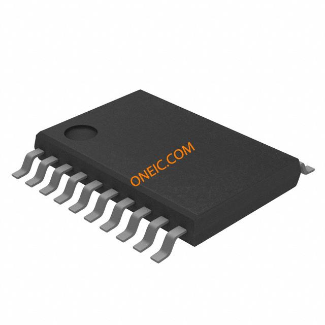
20-TSSOP

Image Preview