74LVC1G126SE-7
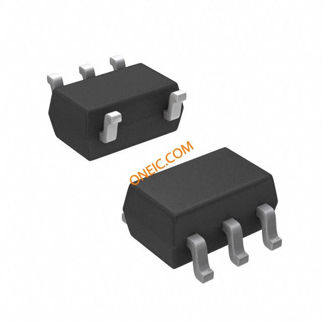
Single-channel non-inverting CMOS buffer drivers in SOT353 package
Manufacturer: ['diodes', 'diodeszetex', 'diodes-zetex']
series introduction
# Introduction to the 74LVC1G126SE - 7 Product Series
## 1. Overview
The 74LVC1G126SE - 7 belongs to a family of single - gate logic devices that are designed to meet the requirements of modern digital circuits. These devices are part of the low - voltage complementary metal - oxide - semiconductor (LVC) technology, which offers a combination of high - speed performance, low power consumption, and excellent noise immunity.
## 2. Key Features
### 2.1 Low - Voltage Operation
- The 74LVC1G126SE - 7 is optimized for operation at low supply voltages, typically ranging from 1.65V to 5.5V. This wide voltage range makes it suitable for use in a variety of applications, including battery - powered devices where power efficiency is crucial. Low - voltage operation also helps in reducing power dissipation, which in turn extends the battery life of portable devices.
### 2.2 High - Speed Performance
- With its advanced LVC technology, the device can achieve high propagation speeds. This allows for rapid data transfer and processing within digital circuits. The fast switching times enable the 74LVC1G126SE - 7 to handle high - frequency signals, making it ideal for applications such as high - speed data communication systems and clock distribution networks.
### 2.3 Tri - State Output
- One of the most significant features of the 74LVC1G126SE - 7 is its tri - state output. The tri - state output can be in one of three states: high, low, or high - impedance. In the high - impedance state, the output effectively disconnects from the circuit, allowing multiple devices to share a common bus without interfering with each other. This feature is essential in bus - based systems, where multiple components need to communicate over a shared data line.
### 2.4 ESD Protection
- The device is equipped with electrostatic discharge (ESD) protection on all inputs and outputs. ESD protection helps to safeguard the device from damage caused by static electricity, which can be a common problem in electronic environments. This protection ensures the reliability and longevity of the 74LVC1G126SE - 7, especially in applications where the device may be exposed to handling or environmental factors that could generate static charges.
### 2.5 Compatibility
- The 74LVC1G126SE - 7 is compatible with both TTL (Transistor - Transistor Logic) and CMOS (Complementary Metal - Oxide - Semiconductor) input levels. This compatibility allows for easy integration into existing digital circuits that may use different logic families. It provides designers with flexibility when upgrading or expanding their systems.
## 3. Functional Description
### 3.1 Logic Function
The 74LVC1G126SE - 7 is a single - gate buffer with a tri - state output. The input signal is passed through the buffer and appears at the output when the output enable (OE) input is active. When the OE input is low, the output is enabled, and the output state follows the input state. When the OE input is high, the output goes into the high - impedance state.
### 3.2 Pin Configuration
- The device typically comes in a small - outline package, which is suitable for surface - mount technology (SMT) assembly. The pins are clearly labeled for easy identification. The input pin is used to receive the logic signal, the output pin provides the buffered signal, and the OE pin controls the output state.
## 4. Applications
### 4.1 Data Communication
- In data communication systems, the 74LVC
Images for reference

SOT-353

Image Preview

Image Preview