74LCX244WMX
Low voltage CMOS buffers and line drivers for signal management
Manufacturer: ['fairchild', 'rochester', 'onsemi']
series introduction
# Introduction to the 74LCX244WMX Product Series
## 1. Overview
The 74LCX244WMX is a member of the advanced logic family of integrated circuits. It belongs to the octal buffer and line driver category, designed to provide high - performance signal buffering and driving capabilities in a wide range of digital systems. This product series is well - known for its low power consumption, high - speed operation, and compatibility with various digital interfaces, making it a popular choice among designers in different industries.
## 2. Key Features
### 2.1 Low Power Consumption
One of the most significant features of the 74LCX244WMX is its low power consumption. It operates on a supply voltage range of typically 2.7V to 3.6V, which is suitable for battery - powered devices and other applications where power efficiency is crucial. The low power design helps to extend the battery life of portable devices and reduces the overall power dissipation in larger systems, leading to cost savings and improved reliability.
### 2.2 High - Speed Operation
The 74LCX244WMX offers high - speed performance with typical propagation delays in the range of a few nanoseconds. This allows it to handle high - frequency signals effectively, making it suitable for applications such as high - speed data transfer, clock distribution, and signal buffering in fast - paced digital systems. The fast switching times ensure that the device can keep up with the rapid changes in input signals, minimizing signal distortion and ensuring accurate data transmission.
### 2.3 Wide Input and Output Voltage Compatibility
It has wide input and output voltage compatibility, which enables it to interface with different logic families. The input thresholds are designed to be compatible with both TTL (Transistor - Transistor Logic) and CMOS (Complementary Metal - Oxide - Semiconductor) levels. This flexibility allows the 74LCX244WMX to be easily integrated into existing systems that use different logic standards, providing a seamless connection between various components.
### 2.4 Output Enable Function
The device is equipped with an output enable (OE) function. The OE pins can be used to control the output state of the buffers. When the OE input is active (low in most cases), the outputs are enabled, and the input signals are passed through to the outputs. When the OE input is inactive (high), the outputs are in a high - impedance state, effectively isolating the device from the rest of the circuit. This feature is useful for bus sharing applications, where multiple devices need to share a common data bus.
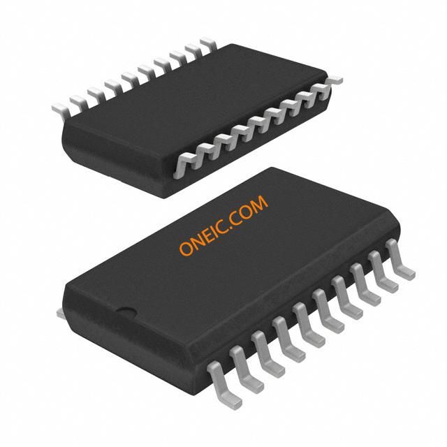
## 3. Pin Configuration and Functionality
### 3.1 Pinout
The 74LCX244WMX is typically available in a small - outline package, such as the TSSOP (Thin Shrink Small - Outline Package). It has a total of 20 pins, which are divided into input pins, output pins, power supply pins, and control pins.
- **Input Pins**: There are eight input pins (A1 - A8), which receive the input signals that need to be buffered and driven.
- **Output Pins**: Corresponding to the input pins, there are eight output pins (Y1 - Y8), which provide the buffered and amplified versions of the input signals.
- **Power Supply Pins**: The VCC pin is used to supply the positive power voltage, and the GND pin is connected to the ground.
- **Control Pins**: There are two output enable pins (OE1 and OE2), which are used to control the output state of the device.
### 3.2 Functionality
The basic functionality of the 74LCX244WMX is to buffer and
Images for reference

20-SOIC 0.295
20-SOIC 0.295
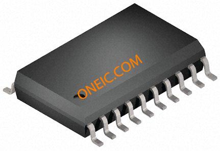
Image Preview