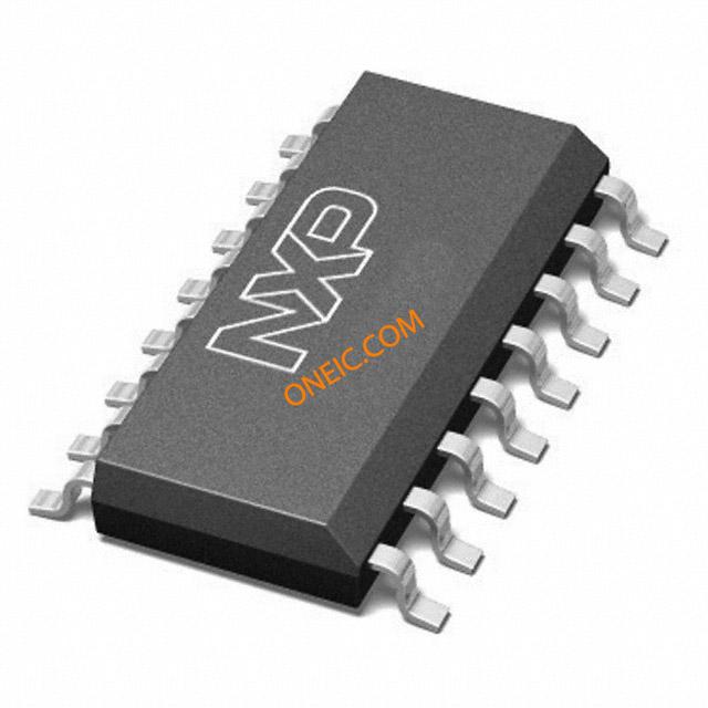
74HCT595D,112
8-bit shift registers for serial to parallel data conversion
Manufacturer: ['nexperia', 'peria', 'nxp']
series introduction
# Introduction to the 74HCT595D,112 Product Series
## 1. Overview
The 74HCT595D,112 is a highly versatile and widely used integrated circuit (IC) belonging to the 74HCT family. This product series is designed to provide an efficient solution for expanding the number of output pins in digital systems. It combines the advantages of high - speed operation and compatibility with both TTL (Transistor - Transistor Logic) and CMOS (Complementary Metal - Oxide - Semiconductor) logic levels, making it suitable for a broad range of applications.
## 2. Key Features
### 2.1 Serial - to - Parallel Conversion
One of the most significant features of the 74HCT595D,112 is its ability to convert serial data into parallel output. It has a shift register that can accept data serially, one bit at a time. This is extremely useful in systems where there is a limited number of available output pins on a microcontroller or other digital device. By using the 74HCT595D,112, multiple output signals can be controlled with just a few input lines.
### 2.2 8 - Bit Output
The IC provides 8 parallel output pins (Q0 - Q7). These outputs can be used to drive various loads such as LEDs, relays, or other digital components. The ability to control 8 outputs simultaneously makes it ideal for applications like LED displays, where multiple LEDs need to be illuminated in a specific pattern.
### 2.3 Storage Register
In addition to the shift register, the 74HCT595D,112 has a storage register. Once the serial data has been shifted into the shift register, it can be transferred to the storage register with a single clock pulse. This allows for the data to be held stable at the outputs while new data is being shifted into the shift register.
### 2.4 High - Speed Operation
The 74HCT595D,112 is designed for high - speed operation. It can handle clock frequencies up to a certain limit (specified in the datasheet), enabling it to keep up with fast - paced digital systems. This high - speed capability makes it suitable for applications that require rapid data transfer and processing.
### 2.5 TTL and CMOS Compatibility
It is compatible with both TTL and CMOS logic levels. This means that it can be easily interfaced with a wide variety of digital devices, regardless of whether they use TTL or CMOS logic. This compatibility simplifies the design process and allows for greater flexibility in system integration.
### 2.6 Output Enable Control
The IC has an output enable (OE) pin. When this pin is pulled low, the outputs are enabled, and the data stored in the storage register is presented at the output pins. When the OE pin is pulled high, the outputs are disabled, and they go into a high - impedance state. This feature can be used to control when the outputs are active, which is useful in applications where multiple devices share the same output lines.
## 3. Pin Configuration
### 3.1 Input Pins
- **SER (Serial Input)**: This is the pin where the serial data is input into the shift register. Data is shifted in on the rising edge of the shift clock.
- **SRCLK (Shift Register Clock)**: The clock signal for the shift register. Each rising edge of this clock causes the data at the SER pin to be shifted into the shift register.
- **RCLK (Storage Register Clock)**: The clock signal for the storage register. A rising edge on this clock transfers the data from the shift register to the storage register.
- **SRCLR
Images for reference

16 SOIC

16-SOIC

Image Preview