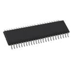
74FCT16244ATPAG
16-channel non-inverting CMOS buffer/line driver in 48-pin TSSOP package
Manufacturer: ['integrated-device-technology', 'idt']
series introduction
# Introduction to the 74FCT16244ATPAG Product Series
## 1. Overview
The 74FCT16244ATPAG belongs to the 74FCT logic family, which is well - known for its high - speed performance and compatibility with a wide range of digital systems. This particular product is a 16 - bit buffer/line driver with 3 - state outputs, designed to provide efficient signal buffering and driving capabilities in various electronic applications.
## 2. Key Features
### High - Speed Operation
One of the most prominent features of the 74FCT16244ATPAG is its high - speed performance. It is capable of operating at clock frequencies that meet the demands of modern digital systems. This high - speed operation allows for rapid data transfer between different components in a circuit, reducing latency and improving overall system efficiency. For example, in high - speed data acquisition systems, the fast switching times of this buffer can ensure that data is accurately and quickly transferred from sensors to processing units.
### 3 - State Outputs
The 3 - state outputs of the 74FCT16244ATPAG provide an additional level of flexibility in circuit design. In the high - impedance (Hi - Z) state, the outputs are effectively disconnected from the circuit, allowing multiple devices to share the same bus without interference. This is crucial in bus - based systems where multiple components need to communicate over a common data path. For instance, in a multi - processor system, the 3 - state outputs enable different processors to take turns accessing the shared data bus.
### Wide Operating Voltage Range
The device can operate over a relatively wide voltage range, typically from 4.5V to 5.5V. This wide voltage tolerance makes it compatible with a variety of power supply configurations, allowing it to be easily integrated into different electronic systems. Whether it is a battery - powered device or a system powered by a regulated power supply, the 74FCT16244ATPAG can adapt to the available voltage levels.
### Low Power Consumption
Despite its high - speed operation, the 74FCT16244ATPAG is designed to consume relatively low power. This is achieved through advanced semiconductor manufacturing processes and circuit design techniques. Low power consumption is beneficial in applications where power efficiency is a concern, such as portable electronic devices. It helps to extend the battery life of these devices and reduces the overall heat generation, which in turn improves the reliability of the system.
## 3. Pin Configuration and Functionality
### Pin Layout
The 74FCT16244ATPAG comes in a specific package with a well - defined pin layout. The pins are divided into input pins, output pins, control pins, and power supply pins. The input pins are used to receive the data signals that need to be buffered and driven. The output pins provide the buffered and amplified versions of the input signals. The control pins, such as the output enable pins, are used to control the operation of the device, specifically to enable or disable the 3 - state outputs.
### Functionality of Control Pins
There are two output enable pins (OE1# and OE2#) in the 74FCT16244ATPAG. When these pins are in the active low state (logic 0), the outputs are enabled, and the input signals are passed through to the outputs. When the output enable pins are in the high state (logic 1), the outputs enter the high - impedance state, effectively disconnecting them from the circuit.
## 4. Applications
### Computer Systems
In computer systems, the 74FCT16244ATPAG can be used as a buffer between different components such as the CPU
Images for reference

Image Preview