74AUP1Z125GW
Low-power crystal drivers for signal buffering and line driving
Manufacturer: ['nexperia', 'nxp']
series introduction
# Introduction to the 74AUP1Z125GW Product Series
## 1. Overview
The 74AUP1Z125GW is a member of a high - performance, low - voltage single - gate buffer/line driver integrated circuit product series. These devices are designed to meet the requirements of modern electronic systems, which demand high - speed operation, low power consumption, and compact form factors. They are commonly used in a wide range of applications, from portable consumer electronics to industrial control systems.
## 2. Key Features
### 2.1 Low Voltage Operation
- The 74AUP1Z125GW is optimized for low - voltage operation, typically operating at supply voltages as low as 0.8V and up to 3.6V. This makes it ideal for battery - powered devices, where minimizing power consumption is crucial. The ability to operate at such low voltages helps to extend the battery life of portable electronics, such as smartphones, tablets, and wearables.
### 2.2 High - Speed Performance
- Despite its low - voltage operation, the product series offers high - speed signal propagation. It has a fast propagation delay, which allows for quick transmission of digital signals. This high - speed performance is essential in applications where real - time data processing and signal transfer are required, such as in high - speed data communication interfaces and high - frequency clock distribution systems.
### 2.3 Small Package Size
- The 74AUP1Z125GW is available in a very small package, such as the SOT - 353 or similar ultra - small packages. This compact form factor is beneficial for printed circuit board (PCB) design, especially in applications where space is limited. It enables designers to create more densely packed circuits, reducing the overall size of the electronic device.
### 2.4 Low Power Consumption
- In addition to its low - voltage operation, the series has low static and dynamic power consumption. The low static power consumption ensures that the device consumes minimal power when in standby or idle mode, while the low dynamic power consumption reduces power usage during active operation. This makes it an energy - efficient choice for a variety of applications.
### 2.5 ESD Protection
- The 74AUP1Z125GW is equipped with electrostatic discharge (ESD) protection. This protection helps to safeguard the device from damage caused by electrostatic discharges, which are common in many electronic environments. It enhances the reliability and durability of the product, reducing the risk of failure due to ESD events.
## 3. Functional Description
### 3.1 Buffer/Line Driver Function
- The primary function of the 74AUP1Z125GW is to act as a buffer or line driver. It takes an input signal and provides a high - impedance output that can drive a load without significantly affecting the input signal. This is useful in situations where a signal needs to be transmitted over a long distance or where multiple loads need to be driven from a single source.
### 3.2 Enable Function
- The device has an enable input (EN). When the enable input is active (usually low - active), the buffer/line driver is enabled, and the output follows the input signal. When the enable input is inactive, the output is in a high - impedance state, effectively disconnecting the output from the circuit. This enable function allows for easy control of the signal flow and can be used for power management and signal isolation purposes.
## 4. Applications
### 4.1 Portable Consumer Electronics
- In smartphones, tablets, and smartwatches, the 74AUP1Z125GW can be used for signal buffering and level shifting. It helps to ensure reliable signal transmission between different components, such as the
Images for reference

SOT-363 PKG
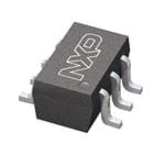
Image Preview

Image Preview