74AUP1T34GW,125
Low-power voltage level translators and buffers in compact 5-pin TSSOP format
Manufacturer: ['nexperia', 'nxp']
series introduction
# Introduction to the 74AUP1T34GW,125 Product Series
## 1. Overview
The 74AUP1T34GW,125 belongs to a specialized family of semiconductor products that play a crucial role in modern electronic circuits. These devices are designed to offer high - performance signal processing and logic control capabilities in a compact and efficient package. They are part of the single - gate logic series, which are widely used in various applications due to their simplicity and flexibility.
## 2. Key Features
### 2.1 Low Power Consumption
One of the most significant features of the 74AUP1T34GW,125 is its extremely low power consumption. In today's energy - conscious world, this is a highly desirable trait, especially for battery - powered devices such as smartphones, tablets, and wearable electronics. The low power design helps to extend the battery life of these devices, reducing the frequency of charging and enhancing the overall user experience.
### 2.2 High - Speed Operation
These devices are capable of high - speed signal processing. They have a fast propagation delay, which means that they can quickly respond to input signals and produce the corresponding output. This high - speed operation is essential in applications where real - time data processing is required, such as in high - speed communication systems and data transfer interfaces.
### 2.3 Wide Operating Voltage Range
The 74AUP1T34GW,125 supports a wide operating voltage range. This flexibility allows it to be used in a variety of different power supply environments. Whether it is a low - voltage system for portable devices or a higher - voltage system in industrial applications, these devices can adapt and function effectively.
### 2.4 Small Package Size
The product comes in a small and space - saving package. This is beneficial for printed circuit board (PCB) designers as it allows for more compact and densely populated circuit designs. The small package size also helps to reduce the overall size and weight of the final product, which is particularly important in applications where miniaturization is a key requirement.
## 3. Functional Description
### 3.1 Logic Function
The 74AUP1T34GW,125 is a single - gate buffer. Its primary function is to isolate and amplify input signals. When an input signal is applied, the device will reproduce the same logic state at the output, but with enhanced drive capability. This is useful in situations where the input signal may be weak or needs to be transmitted over a longer distance without significant degradation.
### 3.2 Input and Output Characteristics
The input of the device has a high impedance, which means that it draws very little current from the source of the input signal. This helps to minimize the loading effect on the previous stage of the circuit. The output, on the other hand, has a low impedance, allowing it to drive other components or loads effectively.
## 4. Applications
### 4.1 Consumer Electronics
In consumer electronics such as smartphones, tablets, and smartwatches, the 74AUP1T34GW,125 can be used for signal buffering and level shifting. For example, it can be used to interface between different voltage domains within the device, ensuring proper communication between various components.
### 4.2 Industrial Automation
In industrial automation systems, these devices can be used in control circuits and sensor interfaces. Their high - speed operation and low power consumption make them suitable for applications where real - time monitoring and control are required, such as in factory automation and robotics.
### 4.3 Communication Systems
In communication systems, the 74AUP1T34GW,125 can be used for signal conditioning and buffering in data transmission lines. It helps to ensure the
Images for reference
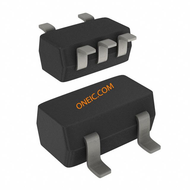
SC-70-5, SC-88A, SOT-323-5, SOT-353, 5-TSSOP
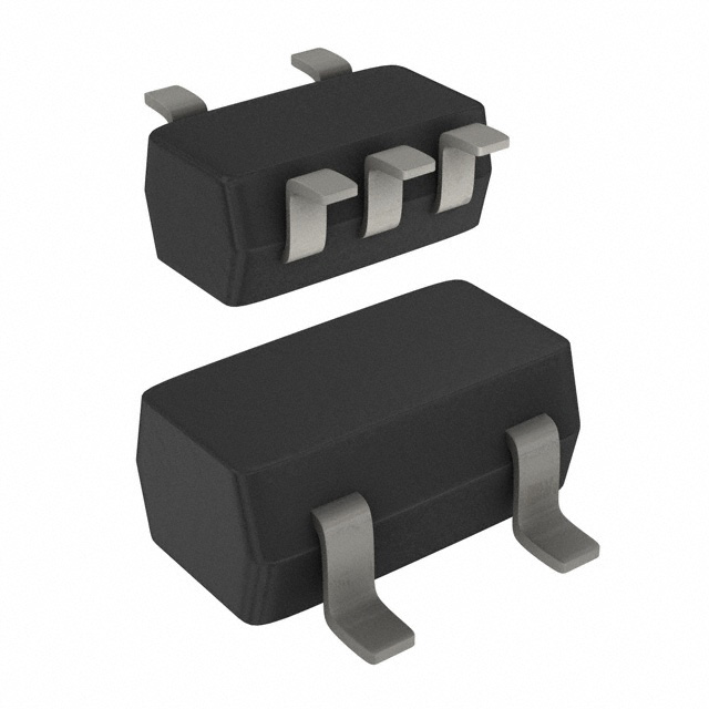
Image Preview
Image Preview