2N7002K-T1-GE3
N-channel MOSFETs, 60V, 0.3A, compact SOT-23 package
Manufacturer: vishay
series introduction
# Introduction to the 2N7002K - T1 - GE3 Product Series
## 1. Overview
The 2N7002K - T1 - GE3 is a significant member of the field - effect transistor (FET) product series. FETs are crucial semiconductor devices widely used in modern electronics due to their unique electrical characteristics. This particular series is designed to meet a variety of application requirements, offering reliable performance and high - quality functionality.
## 2. Product Specifications
### Electrical Characteristics
- **Voltage Ratings**:
- The 2N7002K - T1 - GE3 typically has a drain - source breakdown voltage ($V_{(BR)DSS}$) of around 60V. This high breakdown voltage allows it to handle relatively large voltage differences between the drain and source terminals without suffering from breakdown, making it suitable for applications where higher voltage levels are present.
- The gate - source voltage ($V_{GS}$) has a maximum rating, usually around ±20V. This specification ensures that the device can tolerate a certain range of gate - source voltage without being damaged.
- **Current Ratings**:
- The continuous drain current ($I_D$) is an important parameter. For the 2N7002K - T1 - GE3, it can handle a continuous drain current of up to several hundred milliamperes (e.g., around 200 - 300 mA depending on the operating conditions). This current - handling capacity makes it suitable for driving small - to medium - sized loads.
- The pulsed drain current ($I_{DM}$) is even higher, allowing the device to handle short - duration high - current pulses. This is useful in applications where there are transient current spikes.
- **On - Resistance ($R_{DS(on)}$)**:
- The on - resistance is a key characteristic that determines the power loss in the device when it is in the on - state. The 2N7002K - T1 - GE3 has a relatively low on - resistance, typically in the range of a few ohms (e.g., around 2 - 5 ohms at a specified gate - source voltage and drain current). A low on - resistance means less power is dissipated as heat, resulting in higher efficiency and better overall performance.
### Package and Physical Characteristics
- **Package Type**: It is commonly available in a small - sized surface - mount package, such as the SOT - 23. The SOT - 23 package is widely used in modern electronics due to its compact size, which allows for high - density circuit board designs. It has three leads (drain, source, and gate), making it easy to integrate into various circuit layouts.
- **Dimensions**: The SOT - 23 package has standard dimensions. The length is typically around 2.9 mm, the width is about 1.3 mm, and the height is approximately 1.1 mm. These small dimensions make it suitable for applications where space is limited, such as in portable electronic devices.
## 3. Working Principle
The 2N7002K - T1 - GE3 is an N - channel enhancement - mode MOSFET (Metal - Oxide - Semiconductor Field - Effect Transistor). In an enhancement - mode MOSFET, the channel between the drain and source is initially non - conducting. When a positive voltage is applied to the gate terminal with respect to the source terminal, an electric field is created in the oxide layer of the MOSFET. This electric field attracts electrons to the region beneath the oxide, forming a conducting channel between the drain and source. As the gate - source voltage increases, the conductivity of the channel also increases, allowing more current to flow from the
Images for reference
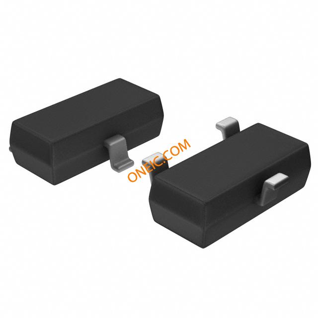
SOT-23-3

SOT-23-3

Image Preview